

Blog
Technical articles on PCB design, manufacturing, and industry best practices. Written by our engineering team.
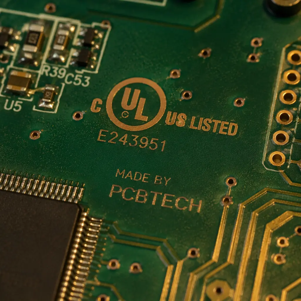
Complete procurement guide to UL certification for PCBs: UL 796 base material standards, UL 94 V-0 flammability ratings, ZPMV2 recognized component marking, how
Complete guide to PCB trace width calculation for current carrying capacity. IPC-2152 vs IPC-2221 comparison, copper weight vs trace width charts, thermal rise
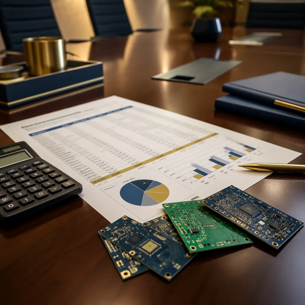
PCB total cost of ownership decoded: the 8 hidden cost drivers beyond unit price, a real TCO formula with 3 sourcing scenarios, and optimization strategies that

Comprehensive guide to PCB thermal management: thermal via design, copper pour strategies, substrate selection, and metal-core PCB solutions. From FR-4 to alumi
Complete PCB thermal management guide: heat sink attachment methods, thermal via arrays, metal-core vs FR-4 selection, and thermal simulation for power electron
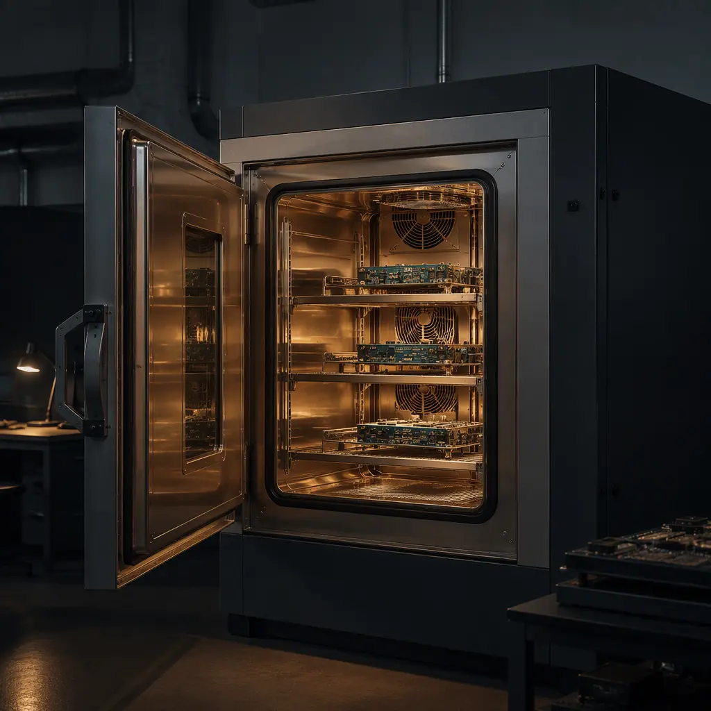
PCB thermal cycling testing guide: IPC-9701 and JESD22-A104 methods, temperature ranges, dwell times, Weibull analysis, solder joint fatigue prediction, and how
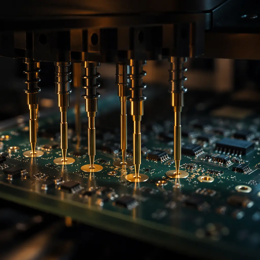
Complete comparison of PCB testing methods: AOI vs X-Ray vs Flying Probe vs ICT vs Functional Test. What each method catches, what it misses, when to use each,

A procurement manager's guide to PCB supply chain resilience: geographic diversification, multi-supplier qualification, tariff engineering, inventory buffers, a

Compare 6 PCB surface finishes — ENEPIG, ENIG, Immersion Silver, Immersion Tin, HASL, OSP — with wire bonding suitability, shelf life data, and cost comparison.

Upload your Gerber files and BOM. We'll respond within 24 hours with a detailed quote and free DFM review.