
Industries / Telecom & 5G
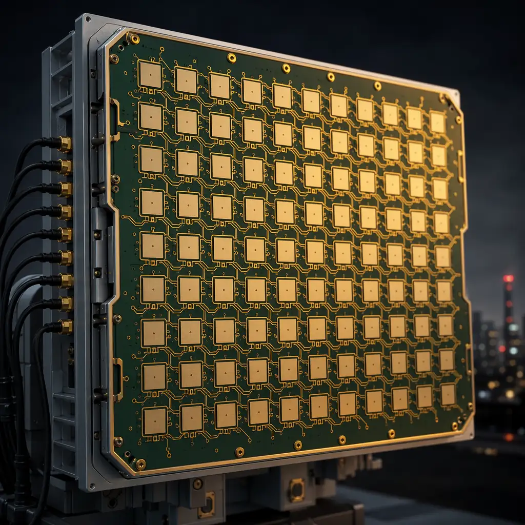
5G AAU beamforming with 64T64R antenna arrays. 800G optical line cards with 32-layer backplanes. Data center switches routing terabits. Rogers, Megtron 6, and Isola high-speed laminates with insertion loss below 0.5dB/in at 28GHz.
Manufacturing Excellence
Up to 32 layers with blind/buried via architecture. Via aspect ratio 10:1 minimum. Registration ±75µm across full panel. For 5G BBU, optical transport, and data center switch backplanes.
Rogers 4350B, 4003C, Megtron 6, Isola Astra MT77. Dk 3.0-3.66 ±0.05 tolerance. Insertion loss <0.5dB/in at 28GHz. Hybrid construction with FR-4 for cost optimization on non-RF layers.
50Ω single-ended, 100Ω differential for SerDes pairs. Up to 112Gbps PAM4 per lane. TDR-verified on every production lot with ±5% tolerance. Back-drilling for stub removal on high-speed via transitions.
0.4mm pitch BGA escape routing for switch ASICs and FPGAs. Via-in-pad with copper-filled and capped laser microvias. 3/3mil trace/space for high-density escape routing.
Back-drilling to remove via stubs on high-speed signal vias (stubs create λ/4 resonance that degrades insertion loss above 10Gbps). Laser depth control ±50µm. For 25-112Gbps SerDes channels.
4-wire Kelvin on 100% of nets. Impedance coupon TDR on every panel. Flying probe for prototypes, bed-of-nails for production. HiPot to 1500V for telecom power supply isolation.
High-Speed Design
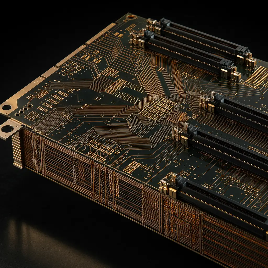
At 112Gbps PAM4, a single bit period is 8.9 picoseconds. Intra-pair skew of 2ps causes a 22% eye closure. For a 32-layer backplane with 14,000+ differential pairs, every pair must be length-matched, every via stub back-drilled, and every impedance transition optimized, or the link budget collapses.
Thermal & Power
A 5G AAU (Active Antenna Unit) mounts on a tower with no fan, ambient to 55°C, solar loading to 85°C surface, and 64 transmit channels collectively dissipating 500-800W. The PCB is the heat sink. Thermal design is inseparable from electrical design.
| Application | Key PCB Demands | Huaxing Solution | Quality |
|---|---|---|---|
| 5G AAU / RRU | RF laminate, thermal, 64ch beamforming, outdoor rated | Rogers+FR-4 hybrid, embedded coin, 32L backplane | IPC Class 3 |
| Baseband Units (BBU) | 32L backplanes, 112G SerDes, 0.4mm BGA | Megtron 6, back-drilling, ±5% impedance | IPC Class 2+ |
| Optical Transport | Mixed-signal, 800G line cards, ultra-low skew | High-Tg FR-4+Megtron hybrid, <1ps intra-pair skew | IPC Class 2+ |
| Data Center Switches | 32-36L, 0.4mm BGA, 112G PAM4, back-drill | Megtron 6, via-in-pad, back-drill ±50µm | IPC Class 2+ |
| Small Cells / DAS | Compact, RF+digital mixed, outdoor, cost-sensitive | 6-10L Rogers hybrid, cavity PCB, conformal coating | IPC Class 2+/3 |
| Satellite Ground Terminals | RF to Ku/Ka band, phased array, harsh environment | Rogers 4350B, metal-core, thermal via grids, polyimide | IPC Class 3 |
5G Infrastructure & Optical
5G deployment spans three domains, radio access (AAU/RRU), fronthaul/backhaul transport, and baseband processing. Each domain has fundamentally different PCB requirements. A 64T64R massive MIMO antenna panel needs 14-18 layers of Rogers 4350B with ±3° phase matching across 64 channels. An 800G optical line card needs 28-32 layers with 112Gbps PAM4 SerDes and <0.5ps intra-pair skew. A single supplier that understands the full signal chain catches integration issues that two separate suppliers never see.
Impedance modeling. Laminate selection for Dk/Df targets. Hybrid construction plan.
Registration ±75µm. Back-drilling ±50µm. Smooth copper on RF layers. Tight Dk laminate.
0.4mm BGA placement. SPI → AOI → X-Ray 100%. Nitrogen reflow. HiPot verification.
TDR on every panel. Insertion loss measurement. VNA to 40GHz for RF coupons.
Thermal cycling -40/+125°C. IST coupon testing. 100% 4-wire Kelvin. Full traceability.
Inside the Factory

At 28GHz, even 2Ω impedance variation causes 5% reflection. Generic "±10% impedance" from a capability sheet is meaningless. Ask for production TDR data at the actual operating frequency.
Via stubs over 50µm create visible insertion loss degradation above 28GHz. Target: ±50µm depth control across full panel with AOI verification of every back-drilled hole.
Laminate Dk variation of ±0.05 (Rogers spec) changes 50Ω impedance by ~2.5Ω. Ask for incoming laminate Dk verification data, not the supplier's certificate, your fabricator's own measurement.
Different CTE between Rogers and FR-4 creates shear stress at the bond line. 500 cycles -40/+125°C with cross-section at 0, 250, 500 cycles. No delamination, no barrel cracking.
At 3.5GHz, a 0.5mm length mismatch between two antenna feed traces creates ~3° of phase error. Across a 64-element array, cumulative phase errors above ±5° degrade beamforming gain by >1dB, equivalent to losing 20% of your cell radius. Ask for: VNA phase measurement on every RF channel of production boards (not just coupon), <±3° phase matching across all 64 channels at 3.5GHz, and end-of-line RF test data showing amplitude and phase per channel. Electrical test passing ≠ phase-matched. A board that passes continuity test can still have 15° of phase error from Dk variation alone.
Insertion loss at 28GHz on FR-4 can be 3× what the simulation predicted because copper surface roughness and Df variation aren't fully modeled. A design targeting <1.5dB total loss from beamformer to antenna element can arrive at 3dB+ on the first build — and you won't know until RF validation. Ask for: VNA S-parameter measurement to 40GHz on production coupons, insertion loss data per lot with pass/fail limits tied to your link budget, and Delta-L or similar de-embedding to isolate PCB loss from connector and launch effects. A shop that quotes "we test to IPC spec" is doing DC continuity test — that tells you nothing about GHz insertion loss.
Send us your stackup, impedance requirements, and board outline. We'll respond within 24 hours with a DFM analysis covering laminate selection, impedance modeling, back-drilling requirements, and thermal management strategy. From a manufacturer that has built telecom PCBs since 2016.

Upload your stackup and signal integrity requirements. We'll respond within 24h with DFM review, impedance modeling, and laminate selection analysis.