

Blog
Technical articles on PCB design, manufacturing, and industry best practices. Written by our engineering team.
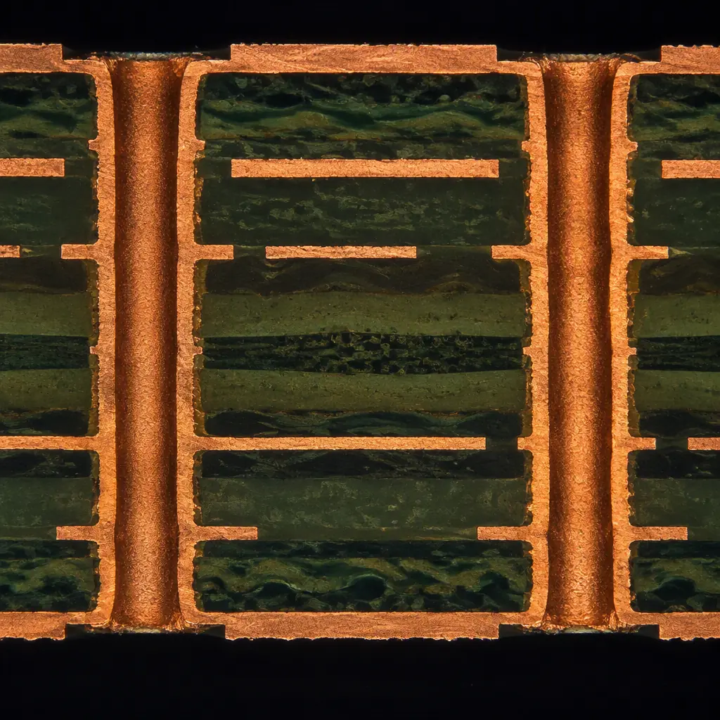
IST, HATS and IPC-TM-650 thermal shock compared — coupons, cycles, runtime, resistance-change criteria and how to choose the right via reliability test for your
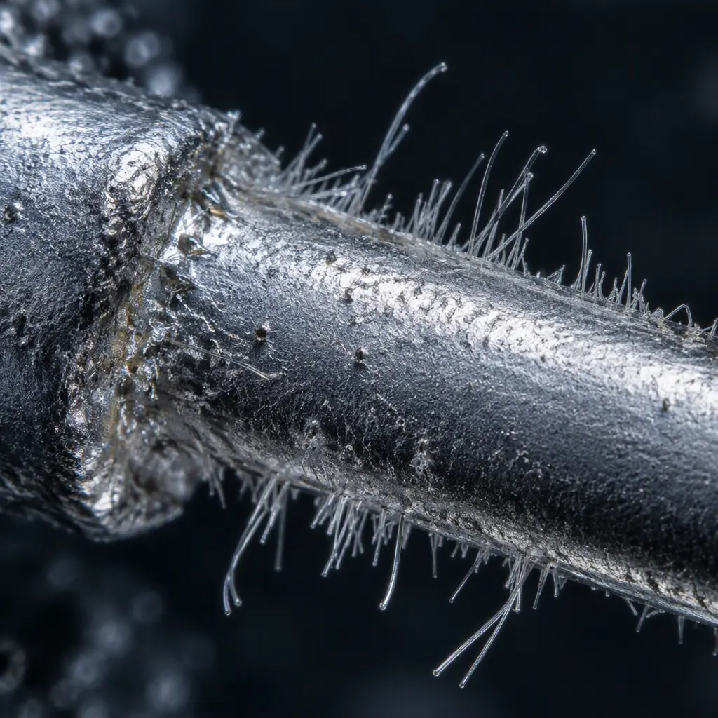
How to specify PCB finishes and processes that suppress tin whiskers — finish propensity table, annealing windows, conformal coating barriers and the spec langu
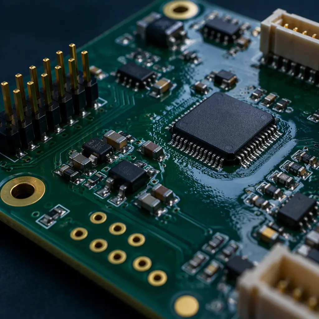
Masking method by coating chemistry decision guide — polyester tape, peelable liquid mask, silicone boots and dispense-only routing, with cost, residue and IPC-

Corner bond, edge bond or full underfill for BGA and CSP — mechanical performance, application time, rework impact and how to choose per package and environment

No-flow underfill process control for high-volume SMT: flux compatibility testing, dispense pattern, void limits, reflow profile interaction and yield economics

How to select and qualify a CSP underfill process: capillary vs no-flow vs molded, dispense patterns, void limits, cure schedules, and the cost per board tradeo
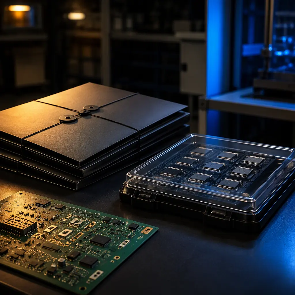
How export control, ITAR and ECCN classification affect PCB and PCBA sourcing from China, the documentation to request, and how to keep controlled designs compl

PCB payment terms for international buyers — T/T deposits, letters of credit, milestone schedules, and how to protect your payment against quality and fraud ris

OEM, ODM and EMS models compared by who owns the design and IP, who carries the risk, and how to choose the right model for a new electronics programme.

Upload your Gerber files and BOM. We'll respond within 24 hours with a detailed quote and free DFM review.