
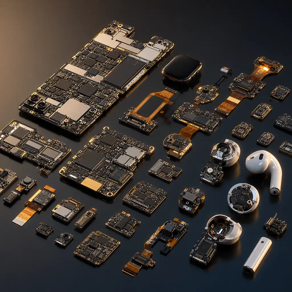
Industries / Consumer Electronics
NPI to 500K/month in 8 weeks. Any-layer HDI with 75µm microvias, 01005 passives, rigid-flex for wearables. 8 SMT lines running 24/6 delivering 8M placements per day, because consumer electronics waits for no one.
Manufacturing Excellence
8 high-speed SMT lines running 24/6. 8M placements per day. Chip shooters for passives, multi-function placers for ICs and connectors. Dual-lane conveyor for parallel production of A/B sides. SPI on 100% of pads before reflow.
75µm laser microvias, stacked and staggered. 0.4mm BGA pitch routing. 0.6mm minimum board thickness for 8-layer any-layer HDI. For smartphones, wearables, and compact IoT devices.
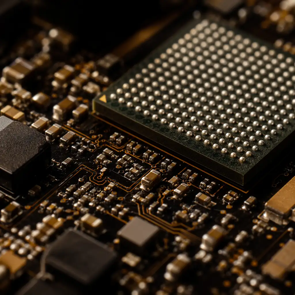
01005 (0.4×0.2mm) passive placement. 0.3mm pitch BGA. 0.4mm pitch QFN. Laser-cut stencil 0.08mm for 01005 pads. Nitrogen reflow. 100% SPI on every pad, no statistical sampling for miniaturized designs.
For wearables, hearables, and foldable devices. Polyimide flex with 0.1mm min bend radius. No-flow prepreg. Bookbinder and window flex configurations. Eliminates connectors, saves space and improves reliability.
NPI prototype in 5 working days. DFM report in 24 hours. Dedicated NPI engineer for each new project. Process validation with first-article inspection report. Ramp from 100 to 500K units/month in 8 weeks.
First-pass yield across all consumer lines. SPC with CpK ≥1.67 on 14 critical parameters. AOI + X-Ray on 100% of boards. 4-wire Kelvin electrical test on 100% of nets. Closed-loop corrective action within 24 hours for any yield excursion.
NPI Excellence
Consumer electronics NPI windows are brutal. Marketing wants launch units for review in 3 weeks. Engineering finds an EMI issue in week 2 that requires a board respin. Operations needs 500K/month by Q4. The PCB partner either keeps pace, or becomes the bottleneck.
Design for Manufacturability
Most PCB DFM reports are auto-generated checklists: "minimum trace width violation at C12 pin 3." That's helpful. What's more helpful: "If you rotate U4 90° and swap L2-L3, you can go from 8 layers to 6 and save $0.47/board." At 500K/year, that's $235,000. Our DFM engineers think in cost and yield, not just design rules.
| Application | Key PCB Demands | Huaxing Solution | Quality |
|---|---|---|---|
| Smartphones & Tablets | Any-layer HDI, 0.4mm BGA, 01005, high volume | 3+N+3 HDI, 75µm microvias, 8 SMT lines, 8M/day | IPC Class 2+ |
| Wearables & Hearables | Rigid-flex, 0.3mm board, 0201/01005, ultra-compact | 8L rigid-flex, 75µm laser vias, cavity PCB, ENIG | IPC Class 2+ |
| Smart Home Devices | BLE/WiFi, 4-8L, cost-sensitive, medium-high volume | 4-8L FR-4, Rogers hybrid for RF, ENIG, volume ramp | IPC Class 2 |
| Laptops & Tablets | 8-12L, rigid-flex display, fine-pitch, high volume | 8-12L HDI, rigid-flex 6L, 0.4mm BGA, ENIG | IPC Class 2+ |
| Gaming & VR/AR | HDI, high-speed, thermal, rigid-flex for headset | 8-12L HDI, Megtron/Rogers for SerDes, metal-core | IPC Class 2+ |
| Power Banks & Chargers | Heavy copper, compact, GaN, high volume | 4-8L, 4-6oz copper, metal-core Al, 4kV HiPot | IPC Class 2 |
Miniaturization & HDI
Consumer electronics miniaturization pushes PCB limits faster than any other industry. Today's flagship smartphone packs 12+ any-layer HDI with 75µm microvias, 0.3mm BGA pitch, and 01005 passives, all on a board thinner than a credit card. Tomorrow's AR glasses and smart rings will be even tighter. Manufacturing at this scale isn't about having the right machines, it's about the process discipline to hold ±15µm registration across 12 layers, every panel, every day.
24h DFM report. Cost optimization analysis. Stackup and impedance modeling. NPI prototype 5 days.
HDI laser drilling. Sequential lamination. ENIG/ENEPIG finish. Impedance coupon on every panel.
01005 placement. SPI 100%. Dual-lane reflow. AOI 100%. X-Ray on BGAs 100%. 8 lines parallel.
NPI→volume transition. Yield monitoring SPC. CpK ≥1.67 on critical dimensions. Continuous improvement.
JIT delivery program. Kanban inventory. Global logistics DDP. 99.2% on-time delivery.
Inside the Factory
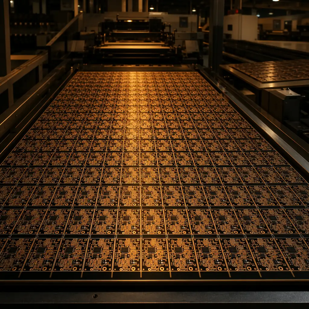
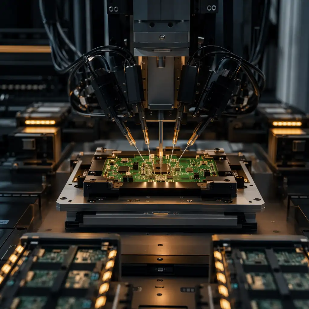
NPI→volume transition is where most shops fail. Lab NPI to volume production is a different process. Ask for a real case study with yield ramp data, not "we can do volume."
Machine spec says 01005. Actual yield depends on stencil, solder paste, placement accuracy, and reflow profile. Ask for: placement yield %, solder void rate (X-Ray data), and tombstoning rate.
Consumer product lifecycles are short. A 12-week component shortage kills the product. Ask about: alternates pre-qualification, allocated stock programs, and BOM risk scoring with mitigation plans.
2% yield drop on 500K/month = 10,000 defective units/month. Response time matters. Ask about: on-site engineering coverage, escalation procedure, and how quickly a closed-loop corrective action starts.
Every manufacturer claims high-volume capability. The proof: ask for a ramp plan that identifies the actual bottleneck at each volume tier. 500→5K: stencil wear and solder paste consistency. 5K→50K: component reel changeover downtime and feeder calibration drift. 50K→500K: panel utilization and multi-line balancing. If they can't name the bottlenecks, they haven't done it.
Consumer products have brutal lifecycle compression. A smartphone model is obsolete in 18 months. Component EOL during production run = costly redesign. Ask about: EOL monitoring with 6-month advance warning, last-time-buy execution at competitive pricing, pre-validated drop-in alternates for all single-source parts, and BOM lifecycle scoring at NPI, red-flagging parts with <24 months to EOL before production starts.
Send us your Gerber files and production forecast. We'll respond within 24 hours with a DFM analysis, cost optimization opportunities, NPI timeline, and volume ramp plan. From a manufacturer with 8 SMT lines already running consumer electronics production.

Upload your Gerber files and production forecast. We'll respond within 24h with DFM, cost optimization, and volume ramp plan.