
Blog
Technical articles on PCB design, manufacturing, and industry best practices. Written by our engineering team.
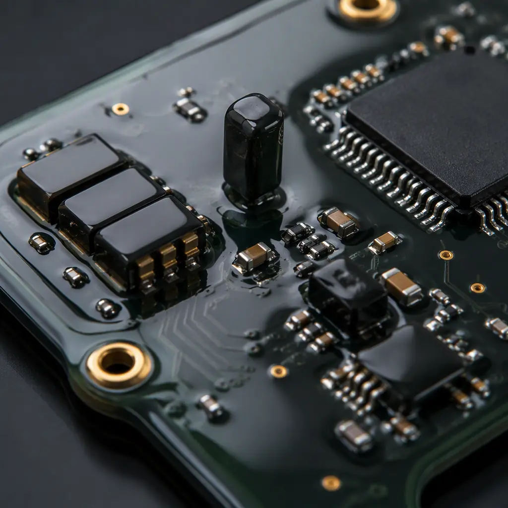
Parylene is the conformal coating that copies the board atom by atom: learn Parylene C/D/N/F types, the thickness range that matters, how vacuum deposition work
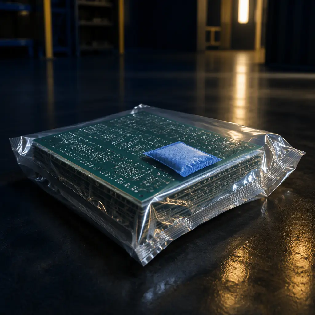
How to store bare PCBs and assembled boards so moisture and corrosion never become a reliability problem: IPC-1601 storage rules, moisture sensitivity level (MS
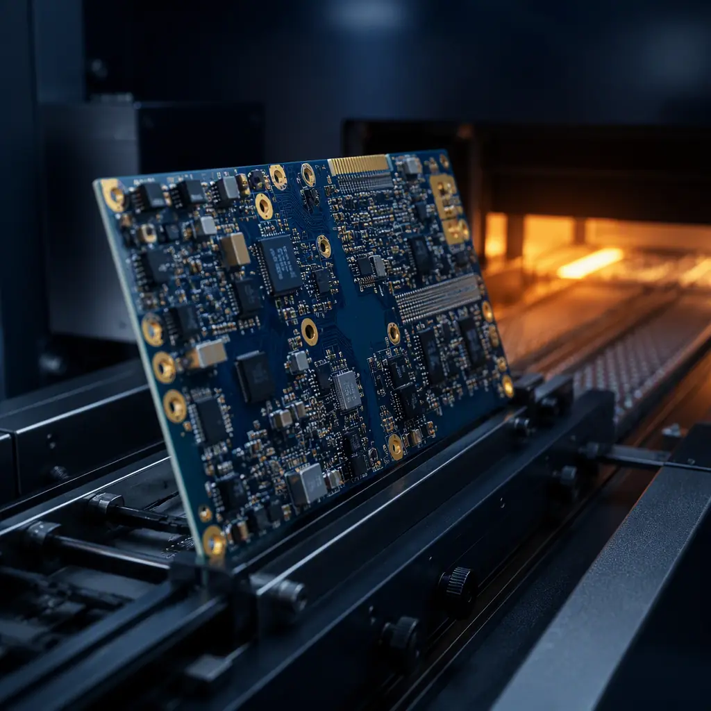
Double-sided SMT and mixed-technology (SMT + through-hole) assembly done right: the reflow order for gluing vs no-gluing, how to handle the second side without
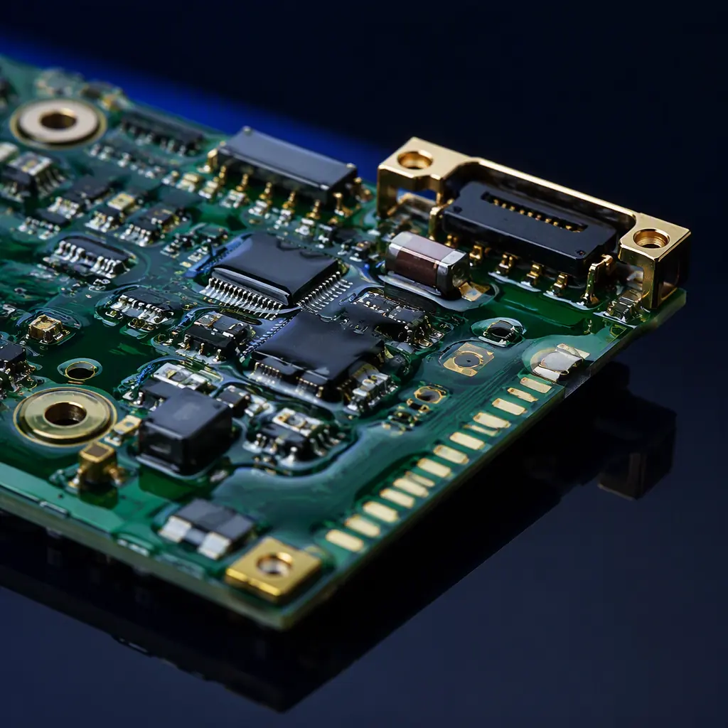
Exactly what IPC-A-610 says a conformal coated board must look like to pass: wet and dry film thickness ranges, void and pinhole limits per Class 1/2/3, coverag
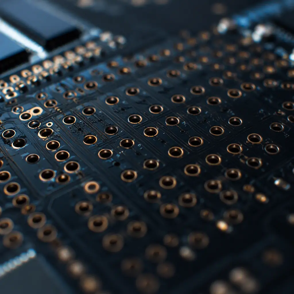
Via aspect ratio is the single most common cause of a via failing a continuity or reliability test. Learn the drill and plating limits for through, blind and mi
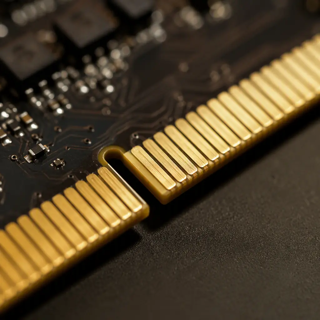
Gold fingers and card-edge connectors are where a PCB meets the system — and where wear, corrosion and poor plating cause field failures. Learn hard gold vs sof
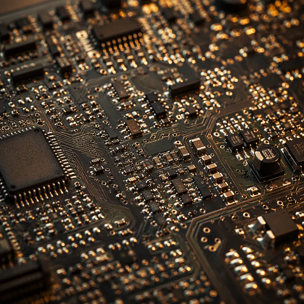
Solder joint defects are the #1 cause of PCBA field failures. Learn the root causes of voids, bridging, cold joints and tombstoning, the IPC-A-610 and J-STD-001
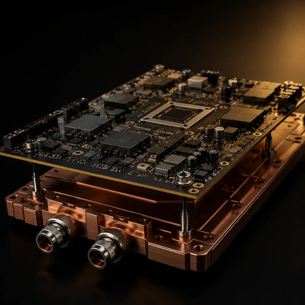
Modern CPUs and GPUs push well past 700 W, and air cooling no longer moves that heat. Learn how cold-plate liquid cooling, copper inlay, heavy copper and therma
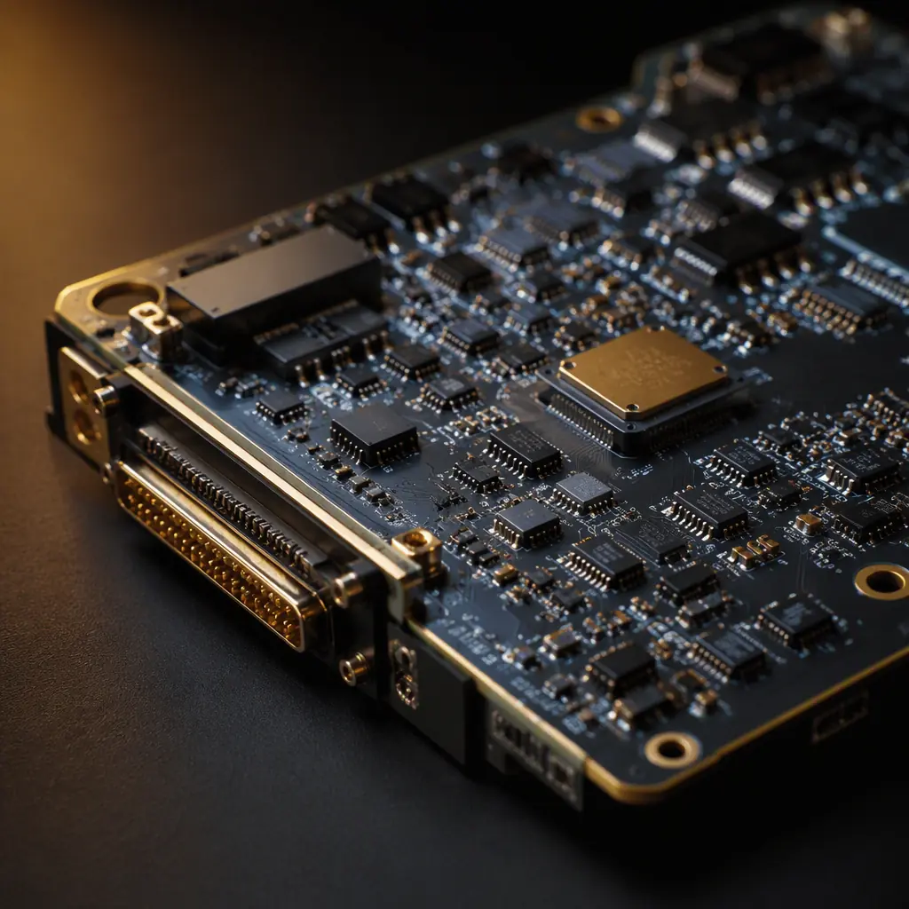
DO-254 governs design assurance for airborne electronic hardware, and the evidence is what makes a board certifiable. Learn the DAL levels A–E, what a DAL A boa

Upload your Gerber files and BOM. We'll respond within 24 hours with a detailed quote and free DFM review.