

Blog
Technical articles on PCB design, manufacturing, and industry best practices. Written by our engineering team.

Wave solder defects trace to five parameters, wave height and alloy condition. Learn the control windows and what to specify on a PO

Wrong or drifted solder alloy causes cold joints, icicles and RoHS failures. Learn how OES and XRF verification work and what to require from a supplier.

Escaped defects reach your line, not the supplier's scrap bin. Learn how to define escape rate, set DPMO acceptance on a PO, and audit AOI/ICT coverage gaps.
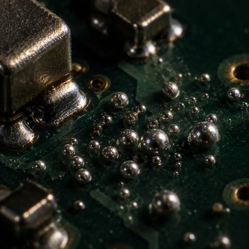
Solder balling and beading cause field failures and rework. Learn the root causes: IPC-based acceptance criteria and an ordered fix path for paste
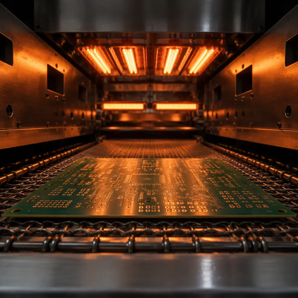
A filed reflow profile is not process control. Learn thermocouple setup, process windows and the PWI — and how to verify a supplier's thermal control

Placement accuracy stats hide the real risk. Learn placement Cpk, and the 7 capability questions to ask an SMT supplier
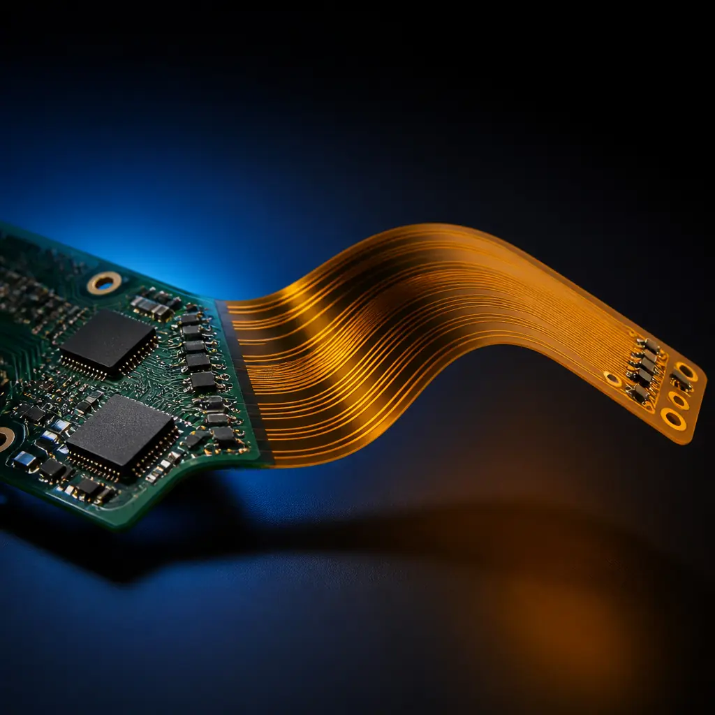
Rigid-flex construction types: stiffeners and the cost drivers behind a hybrid PCB. What to specify before you commit to a build
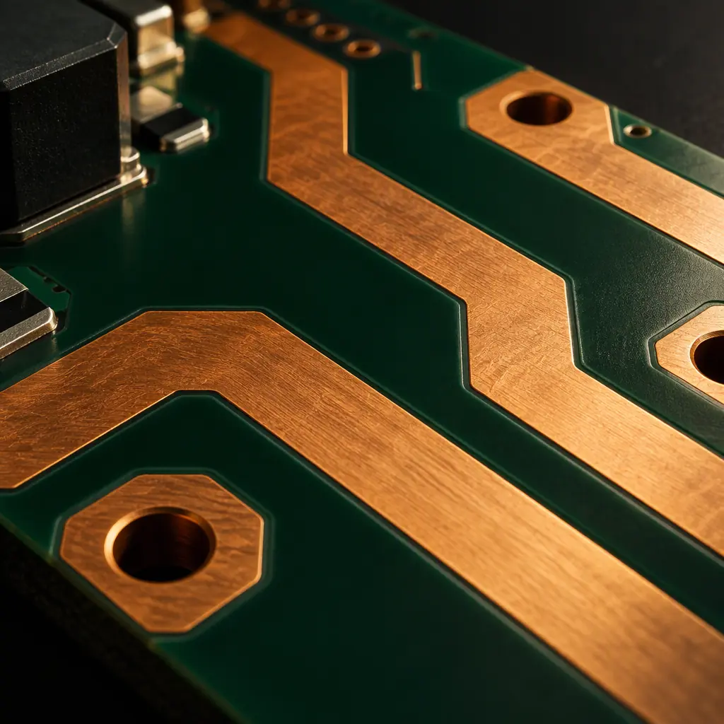
Creepage and clearance spacing tables for high-voltage PCB design: pollution degree, altitude derating, IPC-2221 vs IEC 60664 limits, and coating credit.
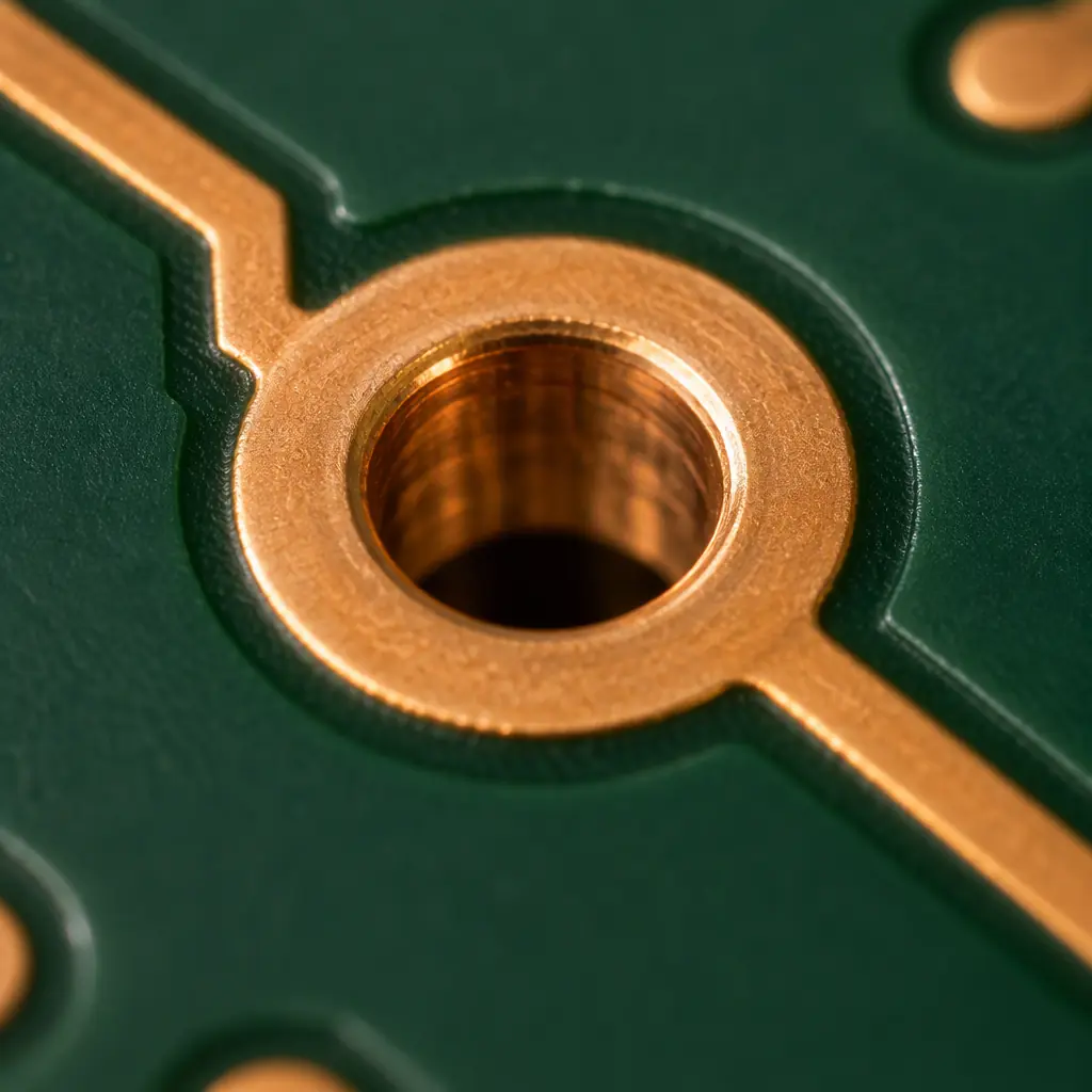
Minimum annular ring by IPC class and how IPC-A-600 grades a breakout. The fabrication spec most quotes assume

Upload your Gerber files and BOM. We'll respond within 24 hours with a detailed quote and free DFM review.