

The moment a board leaves your control, it meets the environment: humidity, salt, airborne dust, thermal cycling, vibration and the fluids of whatever product it lives inside. The question is not whether that environment will stress the board. It is which protective layer you choose, and what you are willing to pay for it.
Three protection families dominate procurement conversations, and a fourth is emerging fast. They are not interchangeable. Each changes the board's thermal profile, its repairability, its testability and its cost per unit in ways that directly affect your warranty exposure. At Huaxing PCBA, conformal coating runs as a standard option across our 8 SMT lines and 4 DIP lines, with parylene and potting available on the same floor under a single ISO 9001 and IATF 16949 quality system. This guide is the comparison you need before you write the protective layer into a purchase order.
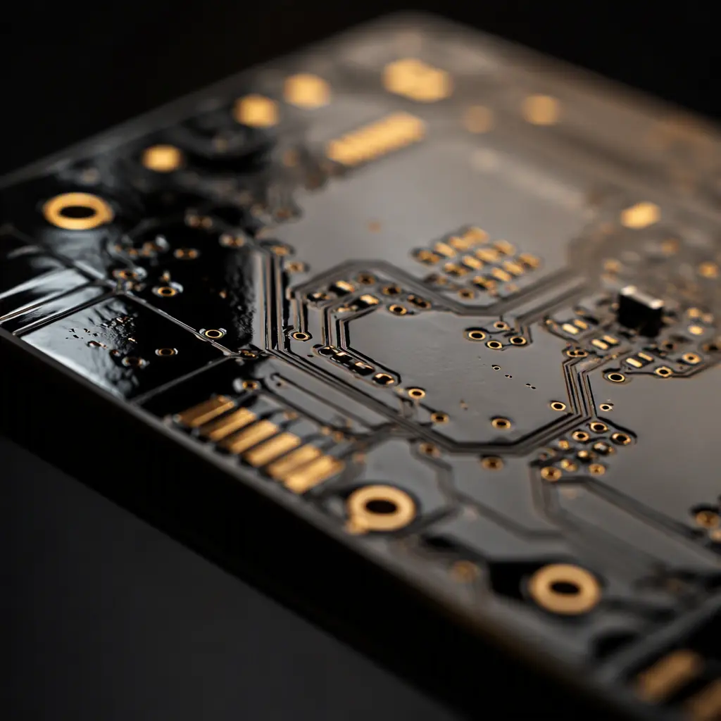
The Four Protection Families a Buyer Actually Chooses Between
The industry uses overlapping terms, but there are four genuinely distinct ways to protect a board, and they differ in material, application method, thickness, and what they reliably protect against.
| Protection | How it is applied | Typical thickness | What it blocks best |
|---|---|---|---|
| Conformal coating | Spray / dip / brush | 25–75 µm | Moisture, condensation, dust, light corrosion |
| Parylene | Vacuum deposition | 0.5–25 µm | Pinhole-free barrier, conformal, high dielectric |
| Potting / encapsulation | Pour / inject, then cure | 1–10 mm | Mechanical shock, vibration, complete moisture seal |
| Nano-coating | Thin-film deposition | 10–200 nm | Hydrophobic surface, mild moisture resistance |
Before comparing them, it is worth naming what part of the board you are actually protecting and why. If the concern is a single exposed BGA or a high-reliability flip-chip, the answer can be underfill rather than a coating at all. If the concern is the whole assembly in a washdown or marine environment, you are likely looking at parylene or potting. See our underfill guide for the solder-joint-specific protection route, which is a different job.
Conformal Coating, What It Covers and What It Does Not
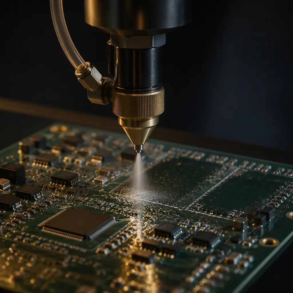
Conformal coating is a thin acrylic, silicone, urethane or epoxy film sprayed over the assembled board. It is the workhorse of industrial, automotive and consumer electronics because it is fast, cheap and easy to remove for rework. Typical aerospace-grade formulations include silicone for high temperature tolerance and urethane for moisture and chemical resistance.
Where it wins
At 25–75 µm it adds negligible thermal resistance and weight, keeps the board repairable, and passes standard IPC-A-610 inspection criteria. It is the default choice for commercial and most industrial products with a moisture or light-corrosion concern.
Where it runs out
A single micro-blister or missed coverage area can let moisture creep in along the board edge and under components. The film is not pinhole-free by nature, and it does little against mechanical shock. For high-reliability automotive or medical, IPC-A-610 Class 3 acceptance demands more rigorous coverage and thickness control. See our IPC-A-610 conformal coating acceptance guide for the criteria that separate a pass from a re-work.
What to verify
Coverage (no bare solder joints or component bodies), thickness in microns, fillet adhesion, and the absence of bubbles. Ask for a documented thickness range and a wet-film check, and confirm the coating is compatible with your connector types. Masked or selective coating is standard on connectors and test points.
Key Takeaway: Conformal coating is the cheapest protection that still looks professional, but it is a barrier against slow environmental ingress, not against mechanical abuse or gross water intrusion. Match it to the real failure mode.
Parylene. When a Thin, Pinhole-Free Vacuum Coat Is Worth It
Parylene is deposited in a vacuum chamber as a monomer that polymerizes directly onto every surface: including under components, inside vias and into tight crevices that spray processes cannot reach. The result is a truly conformal, pinhole-free, optically clear film with excellent dielectric properties and very low outgassing.
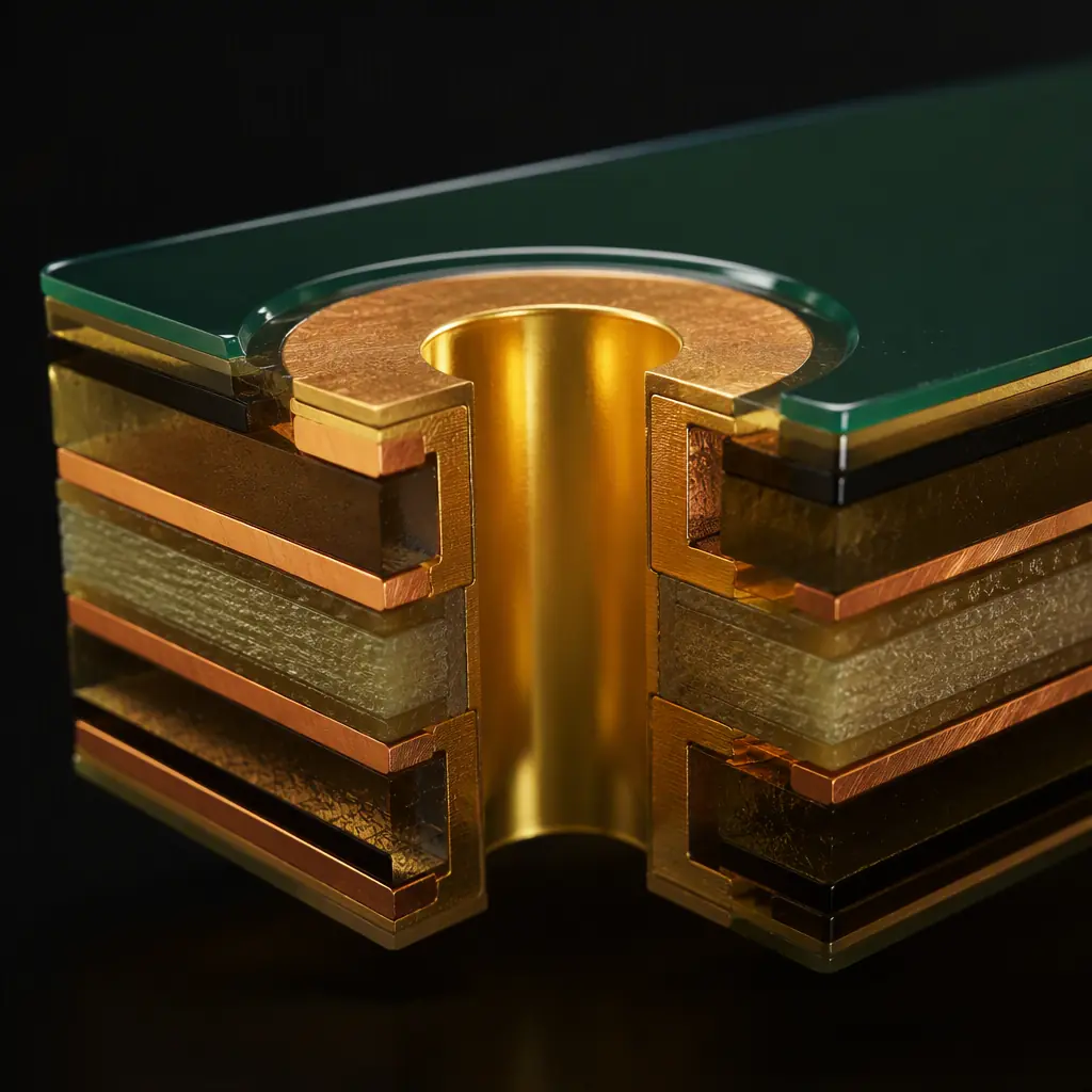
Because the film is only 0.5–25 µm, parylene adds virtually no weight or thermal mass, making it the choice for medical implants, MEMS, aerospace avionics and high-frequency RF boards where any added dielectric or moisture could detune performance. It also protects against the solder-flux residue and ionic contamination that a thicker coating would trap. For the cleanliness side of that equation, read our ionic contamination and cleanliness testing guide.
Trade-Off: Parylene is the hardest to rework. It does not strip with solvent in the way acrylic does, and it is more expensive per board and longer in cycle because it is a batch vacuum process. It is right when the reliability premium is worth it, and wrong when you need field repairability.
Potting and Encapsulation, The Slower, Stronger Route
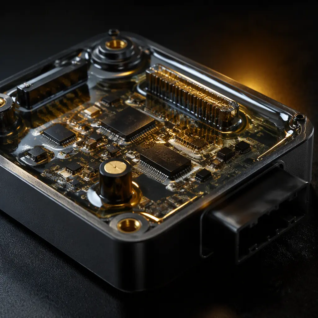
Potting fills a housing around the whole board (or a module) with a two-part resin, polyurethane, silicone or epoxy, that cures into a solid block. It is not a coating; it is a physical encapsulation. At 1–10 mm, it provides true protection against vibration, mechanical shock and complete moisture ingress, and it is what you specify when a board will live inside a pump, a battery pack, an automotive module or an outdoor sensor that gets rained on.
The trade-offs are real: potting adds weight and thermal constraint (the resin conducts heat less well than open air, so power density matters), it is essentially unrepairable, and it makes in-circuit test or probe access impossible after cure. That is why potting is almost always decided at the enclosure-design stage, not as an afterthought. Our potting and encapsulation guide covers resin selection and the thermal design implications in detail.
| Protection | Repairability | Thermal impact | Relative cost per board | Best fit |
|---|---|---|---|---|
| Conformal | High (solvent strip) | Minimal | $ low | Industrial, consumer, most automotive |
| Parylene | Low (special process) | Minimal | $$$ high | Medical implant, aerospace, RF |
| Potting | None (destructive) | Moderate–high | $$ moderate | Vibration, washdown, sealed modules |
| Nano-coating | Moderate | Minimal | $$ moderate | Hydrophobic, light protection add-on |
Nano-Coating, The Emerging Thin-Film Option
Nano-coatings lay down a nanometers-thick hydrophobic layer, usually by vapour deposition or plasma. They are not a substitute for a real barrier. A 10–200 nm film does not stop gross moisture the way parylene or potting does. Their strength is extreme thinness and the ability to repel water and some oils, often applied as a final step on top of a selective conformal coating for connectors and sensitive components. Because the market is still maturing, treat nano-coatings as a targeted enhancement, not a primary protection strategy, and always verify compatibility with your expected corrosion and immersion tests rather than trusting a datasheet.
Coating vs Underfill, Two Different Jobs
A common procurement confusion is treating coating and underfill as alternatives. They are not. Underfill fills the tiny gap between a BGA or flip-chip and the board to stop solder-joint fatigue and cracking from thermal cycling; a coating stops environmental ingress. A high-reliability board often needs both. If your failure mode is cracked joints under thermal cycling, that is an underfill problem, not a coating problem. And if it is moisture, it is the opposite. Our underfill guide explains the selection between capillary, no-flow and molded underfill for the solder-joint question.
A Decision Table for Your Next RFQ
The fastest way to settle this with a supplier is to answer three questions before you send the Gerber files: what is the environment, what is the failure history you are trying to prevent, and what is your service and repair model. The table below turns those answers into a protection call.
| Your situation | Recommended protection | How to state it in the RFQ |
|---|---|---|
| Indoor product, mild humidity | Conformal, acrylic/silicone | Specify material, 25–50 µm, selective on connectors |
| Automotive under-hood or high-vibration | Conformal (silicone) or partial underfill | Specify Class 3 thickness + coverage criteria |
| Medical implant or aerospace, waterproof seal | Parylene | Specify parylene C, thickness, and low-outgassing |
| Sealed outdoor module, washdown, vibration | Potting / encapsulation | Specify resin, cure, and no post-cure thermal exceedance |
| Connectors and test points still need access | Selective coating or masking | State the masked zones in the drawing |
| BGA / flip-chip cracking under thermal cycling | Underfill, not coating | Reference underfill selection criteria |
Key Takeaway: Protection is a decision about cost, repairability and the dominant failure mode, not a default checkbox. State the environment, the failure history and your repair model, and let the supplier quote the material and thickness rather than just a vague "coating" line.
Once the protection is settled, think about the rest of the reliability chain: thermal management, ESD control and testing. Our thermal management guide and ESD control program explain the surrounding measures, and our testing methods article covers the verification that confirms the protection actually works on your lot.
At Huaxing PCBA we run 8 SMT lines, 4 DIP lines and a dedicated conformal-coating station inside our 15,000 m² facility with 500+ staff, processing over 8 million placements per day for customers in 30+ countries. We are ISO 9001, IATF 16949 and UL (E354321) certified, and we document the coating material, thickness and inspection criteria for every lot. Upload your files for a quote or talk to our engineering team about your protection specification.
