
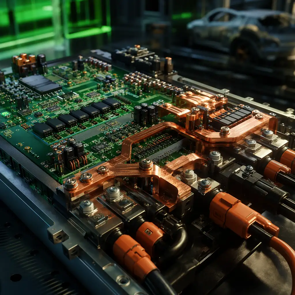
Industries / New Energy
350kW EV chargers switching SiC at 50kHz. 1500V string inverters in desert solar farms. Megawatt-hour BESS containers with 1000VDC bus. Heavy copper to 12oz, 4kV HiPot isolation, IGBT/SiC power stages, from a manufacturer that understands power electronics.
Manufacturing Excellence
6oz inner layers standard for power distribution, 10-12oz for EV charger output stages. 50mm-wide 10oz trace carries 200A continuous with 20°C rise. Selective heavy copper reduces cost ~40% vs. all-layer.
400V to 1500V working voltage designs. Creepage/clearance per IEC 60664 at Pollution Degree 3. Isolation slots with post-routing debris wash. HiPot verification on 100% of production boards.
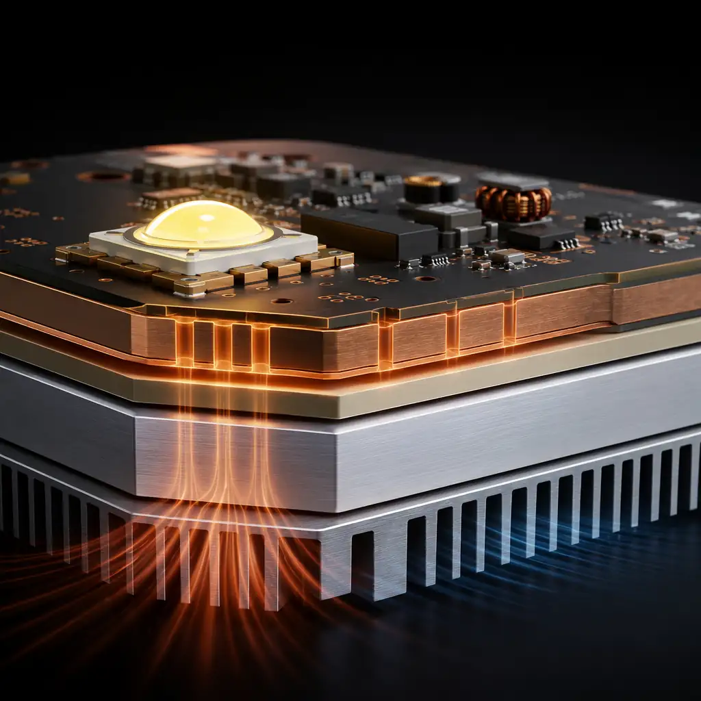
Aluminum or copper base 1.5-3.0mm for direct heat sinking. Dielectric thermal conductivity 1-3 W/m·K vs. 0.3 W/m·K for FR-4. For LED drivers, DC-DC converters, and motor controller power stages.
1500V system voltage designs. CTI ≥600V laminate for 1000VDC+ bus. 4kV HiPot between primary and secondary. Conformal coating for outdoor/desert installation. 25-year design life.
Battery management system (BMS) with precision voltage sensing (±0.1%). 1000VDC bus isolation. Daisy-chain or isoSPI interconnects for stackable modules. UL 1973 / IEC 62619 compliant.
Power layers at 6-10oz copper, signal layers at 1-2oz, all in single lamination. IMS (Insulated Metal Substrate) for direct-bonded power devices. Via aspect ratio 8:1 maintained on heavy copper layers.
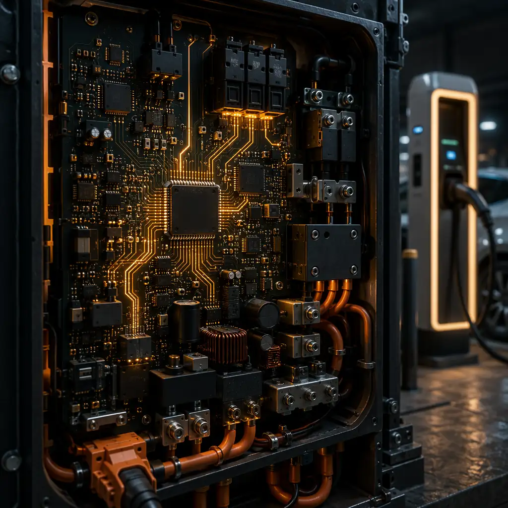
EV Charger Power Stage
A 350kW DC fast charger delivers 500A at 800V through the PCB. At 97% efficiency, that's 10.5kW of heat to dissipate. The PCB is simultaneously a current bus, a heat spreader, a high-voltage isolator, and a precision gate-drive signal router. Every function must coexist without compromise.
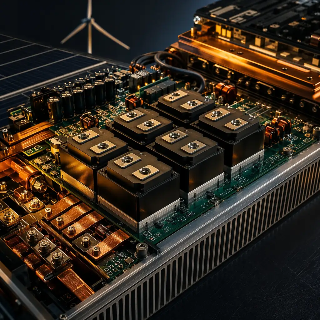
Solar & Storage
A solar microinverter under a panel in Arizona cycles from -20°C to +85°C every day for 25 years. That's 9,125 thermal cycles. Every solder joint, every laminate interface, every conformal coating bond must survive without degradation. Design margin isn't optional, it's the difference between a 2-year warranty claim and a 25-year revenue stream.
| Application | Key PCB Demands | Huaxing Solution | Quality |
|---|---|---|---|
| DC Fast Charger (350kW) | 12oz copper, SiC gate drive, <2nH loop L, embedded coin | 10-12oz, 4kV HiPot, copper coin, planar DC bus | IPC Class 2+ |
| On-Board Charger (OBC) | 6-11kW, compact, high-Tg, automotive qualified | 6-10oz hybrid, high-Tg FR-4, metal-core option | IPC Class 2+ |
| String Inverter (1500VDC) | HV isolation, outdoor rated, 25yr life, thermal cycling | CTI ≥600V, 8mm creepage, conformal coating, polyimide | IPC Class 2+ |
| Microinverter / Optimizer | Compact, under-panel rated, -40 to +85°C, 25yr life | Metal-core, high-Tg, conformal coating, 1000+ cycles | IPC Class 2+ |
| Battery BMS (Residential) | Precision analog, isolation, 16S LiFePO4/NMC | 6-8L, guard rings, isoSPI, ±0.1% voltage sense | IPC Class 2+ |
| Wind Power Converter | Heavy copper, IGBT power stage, HV, harsh environment | 10-12oz, 4kV HiPot, polyimide, embedded coin, 32L | IPC Class 3 |
Thermal Design & Reliability
A 350kW EV charger power stage dissipates 10.5kW at 97% efficiency on a PCB the size of a tablet. Without engineered thermal management, junction temperatures exceed 175°C in under 60 seconds. Every design decision, copper weight, via placement, dielectric thickness, baseplate material, is a thermal decision. Our thermal team runs CFD simulation before fabrication, not as a post-mortem when boards come back from the field.
Heavy copper etch analysis. Creepage/clearance audit per IEC 60664. Thermal via optimization.
Copper-weight-optimized etching. High-Tg or polyimide lamination. Hybrid stackup bonding.
IGBT/SiC module placement. Heavy copper thermal profiling. SPI → AOI → X-Ray on 100%.
4kV HiPot on 100%. Thermal cycling -40/+125°C sample testing. Partial discharge screening.
Conformal coating for outdoor products. Final HiPot verification. 99.2% on-time delivery.
Inside the Factory
Heavy copper (10-12oz) has different CTE mismatch behavior than standard 1oz. Cross-sections at 0, 250, 500, 1000 cycles. No delamination, no barrel cracks, no CAF growth. If they don't have this data, they haven't qualified heavy-copper reliability.
HiPot test on 100% of boards, not sample, not "design verification." 4kV DC for 1 second, leakage <1mA. Isolation slots post-routing washed and inspected before HiPot. Ask for test data from a recent order.
Some components need rework access. Masked connectors, peelable solder mask over test points. Documented re-coating procedure after rework with HiPot re-verification. Not "spray the whole board and hope nothing fails."
Laminated planar bus structure with thin dielectric for low ESL. <5nH total loop inductance from DC link to switching node. Critical for SiC/GaN with >50V/ns dv/dt. Ask for partial discharge test data.
SiC and GaN semiconductors have fewer second-source options than silicon IGBTs. A single Wolfspeed or Infineon part going EOL can halt production for months. Ask about: pre-qualified alternates for every power semiconductor in your BOM, die-level compatibility verification (not just package, gate threshold voltage range, Rds(on), gate charge), and buffer stock program for sole-source SiC parts with 6-month lead time cushion.
1500VDC solar inverter and 1000VDC BESS boards must pass partial discharge testing per IEC 60270. PD inception voltage ≥1.5× rated operating voltage, extinction voltage ≥1.25×. Discharge magnitude <10pC at test voltage — any higher and there's a void or delamination that will grow over 25 years of thermal cycling. This is NOT the same as HiPot — HiPot finds gross isolation failures; PD finds latent defects that HiPot misses and that fail after 5-8 years in the field.
Send us your power stage schematic, voltage/current requirements, and thermal budget. We'll respond within 24 hours with a DFM analysis covering heavy copper feasibility, HiPot isolation strategy, thermal management, and enclosure integration. From a manufacturer that builds power electronics PCBs daily.

Upload your power stage design and voltage/current specs. We'll respond within 24h with DFM review, heavy copper analysis, and HiPot isolation strategy.