
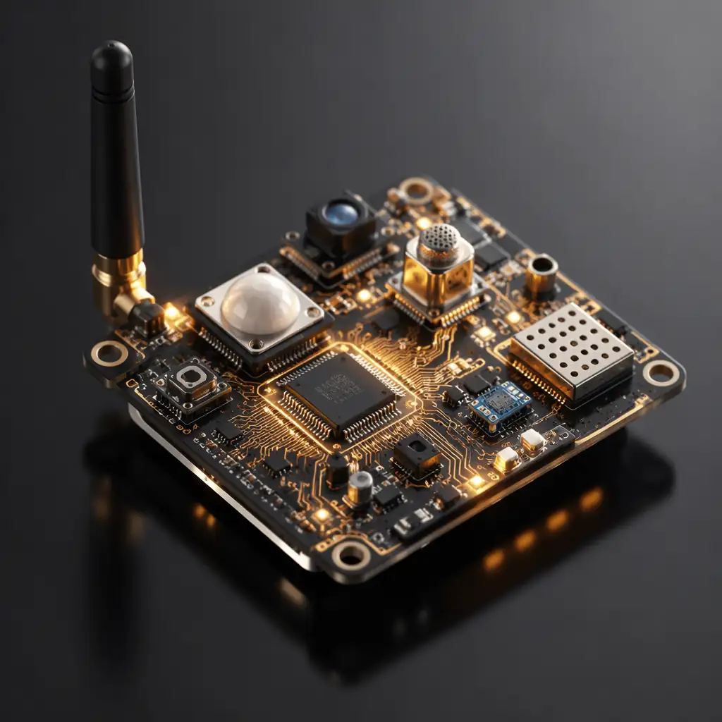
Industries / Internet of Things
Smart sensors in a -30°C cold chain. BLE mesh nodes running 5 years on a coin cell. LoRaWAN gateways on a remote tower. Rigid-flex to 8L, 75µm microvias, Rogers+FR-4 hybrid for antenna-integrated designs.
Manufacturing Excellence
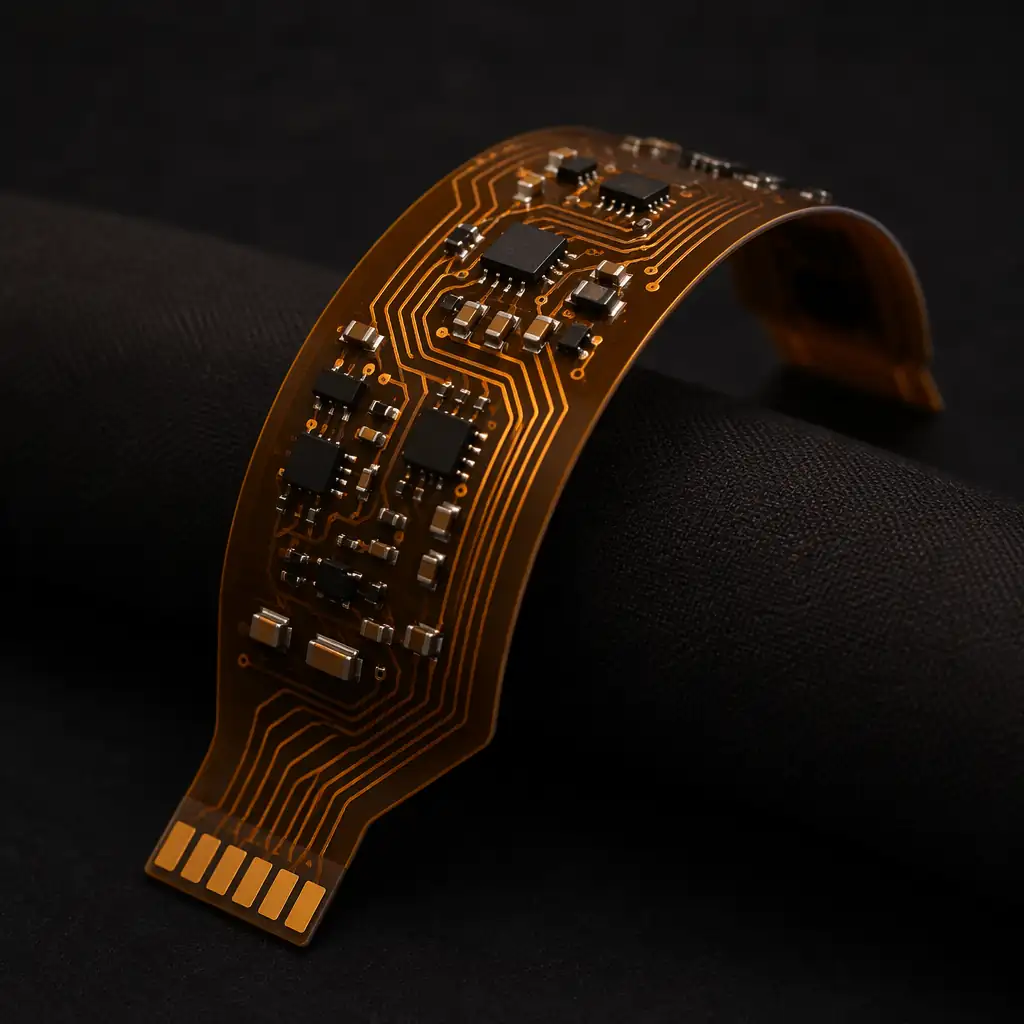
Polyimide flex layers between FR-4 rigid sections. Eliminates connectors and cables, saves 30-50% volume and 40-60% weight. Bookbinder, window, and sculptured flex. 0.1mm min bend radius for dynamic flex.
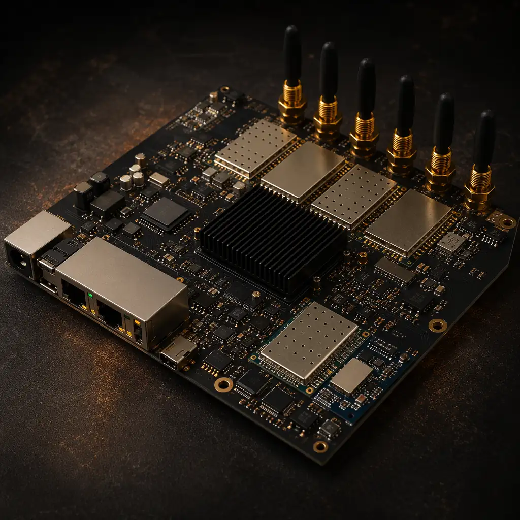
Rogers 4350B, 4003C, Megtron 6 hybrids with FR-4 for antenna-integrated designs. 50Ω and 100Ω differential. TDR-verified on every lot. Insertion loss <0.5dB/in at 5.8GHz for BLE/WiFi.
Stacked and staggered microvias in any-layer HDI. 0.1mm pad size, 0.2mm pitch. Enables 0201 and 01005 passives. 3+N+3 stackup for sensor-to-processor routing in <25×25mm PCB area.
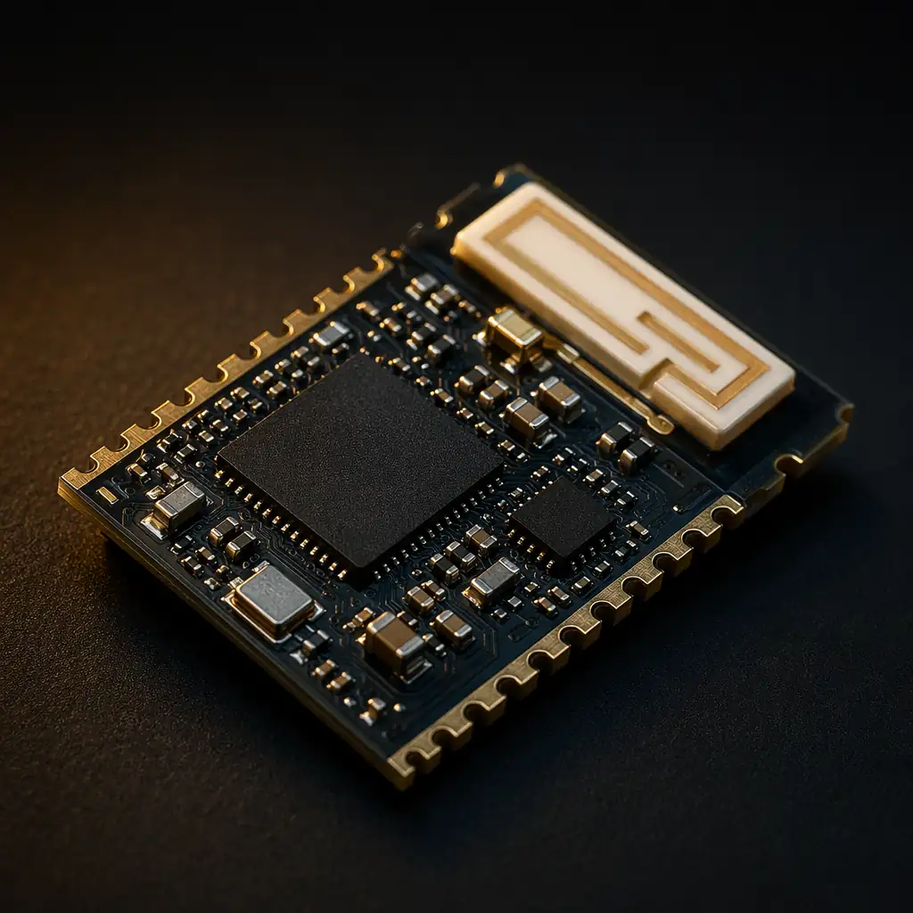
For cellular IoT modules (u-blox, Quectel, SIMCom), BLE SoCs (Nordic nRF52/nRF53), and compact MCU+radio SIPs. 0.4mm BGA pitch routing with 75µm microvias.
Conformal coating for outdoor sensor nodes. ENIG+hard gold edge connectors for battery contacts. Leakage current <1µA verified on every power rail. Suitable for 5+ year coin-cell runtime.
From 100-unit NPI to 500K/yr mass production. 8 SMT lines, 8M placements/day. Consistent quality at scale, SPC with CpK ≥1.67 on all critical dimensions across full production run.
Rigid-Flex Architecture
Every board-to-board connector is a point of failure, adds 15-25mm² of PCB area, consumes 8-15mA of contact resistance, and costs $0.15-1.20 in BOM. Rigid-flex replaces connectors with polyimide flex layers laminated between FR-4 rigid sections.
Wireless Engineering
An antenna-integrated PCB that works on the bench can fail at the EMC lab. Impedance mismatch, ground plane discontinuity, and coupling to nearby traces turn a clean BLE module datasheet into a failing radiated emissions test.
| Application | Key PCB Demands | Huaxing Solution | Quality |
|---|---|---|---|
| Wearables & Hearables | Rigid-flex, microvias, ultra-compact, 0.3mm min | 8L rigid-flex, 75µm laser vias, any-layer HDI | IPC Class 2+ |
| Smart Home Sensors | BLE/Zigbee/Thread, low-power, conformal coating | Rogers+FR-4 hybrid, <1µA leakage, ENIG | IPC Class 2 |
| Cellular IoT Gateways | 4G/5G RF, high-layer routing, GPS integration | 6-12L, Rogers+FR-4, ±5% impedance, 0.4mm BGA | IPC Class 2+ |
| Industrial IoT Nodes | -40°C to +85°C, vibration, sealed enclosure | High-Tg FR-4, conformal coating, heavy copper option | IPC Class 3 |
| Asset Trackers | Multi-radio (GNSS+BLE+LoRa), battery-optimized | 6L Rogers hybrid, 75µm microvias, 0.6mm board | IPC Class 2+ |
| Medical IoT / RPM | Biocompatible, high reliability, 100% test | ENIG, conformal coating, full AOI+X-Ray, traceability | IPC Class 3 |
Impedance stackup verification. Antenna keep-out audit. Ground via placement check.
Rogers+FR-4 single-cycle lamination. Laser microvia drilling. Plated flex vias.
01005 placement capability. SPI → AOI → X-Ray on 100%. Nitrogen reflow for fine-pitch.
TDR impedance test on every lot. Pre-compliance EMC screening. Insertion loss measurement.
From NPI 100 units to 500K/yr. Full traceability. 99.2% on-time delivery.
Miniaturization
An IoT sensor module that's 40×25mm today needs to be 25×18mm for the next generation, same functionality, same battery life, smaller envelope. Miniaturization requires rethinking the entire stackup, component selection, and assembly process.
Inside the Factory
Simulated impedance and measured impedance differ by 3-5% from etch variation and laminate εr tolerance. Ask for TDR data on production lots, not coupon data, not simulation screenshots.
Microvia density creates more glass-resin interfaces, more CAF failure points. CAF-resistant laminate and controlled lamination profile are non-negotiable. Ask for 500-hour CAF test data.
Rigid-flex has unique process challenges: no-flow prepreg cure profile, flex-rigid interface registration, and polyimide via plating. A shop doing 2 orders/month hasn't debugged these processes.
01005 placement needs <25µm placement accuracy, laser-cut 0.08mm stencil, and nitrogen reflow. Acceptable void rate <15% per joint via X-Ray. If they can't show data, they can't assemble 01005s reliably.
An IoT sensor running on a CR2032 coin cell has a total energy budget of ~225mAh. If the PCB leaks 10µA in deep sleep, that's 87.6mAh/year, nearly 40% of the battery wasted on leakage, not sensing. Ask for: power rail leakage measurement (<1µA target) on every production board, conformal coating to prevent humidity-induced leakage current drift, and ENIG surface finish to prevent oxidation that creates leakage paths between closely spaced pads over time.
FCC/CE certification for intentional radiators costs $15-30K per submission. Failing means re-spin + re-test + 4-6 week delay. A PCB partner that ships after "electrical test passed" is leaving $25K of certification risk on your desk. Ask for: conducted emissions pre-scan (CISPR 32 Class B), radiated emissions spot-check at known trouble frequencies, and impedance TDR data showing ±5% on every RF trace. A manufacturer who's shipped wireless products knows the difference between "test passed" and "will pass at the EMC lab."
Send us your stackup requirements, RF bands, and mechanical envelope. We'll respond within 24 hours with a DFM analysis covering impedance control, rigid-flex feasibility, miniaturization options, and volume ramp planning, from a manufacturer that ships IoT PCBs daily.

Upload your Gerber files and RF requirements. We'll respond within 24h with DFM review, impedance analysis, and rigid-flex feasibility.