

Blog
Technical articles on PCB design, manufacturing, and industry best practices. Written by our engineering team.
How to control PCB waivers and deviations: the difference between them, which defects can be conceded and which never can, who signs at what value

How PCB capacity reservation actually works: what a supplier can and cannot commit, the difference between reserved SMT hours and reserved panel area
How to run a PCB golden sample approval that survives production: which build becomes the reference, what the sign-off covers, retention rules

Thermal via array design rules for QFN and power packages: via count vs drill size, filled vs tented vias, thermal relief spokes
Solder paste printability depends on viscosity, metal content and slump rather than one viscosity figure. What each test measures and how to specify paste
How to specify PCB solder mask: LPI vs dry film vs UV ink, on-trace thickness for impedance and solder dams, registration tolerance
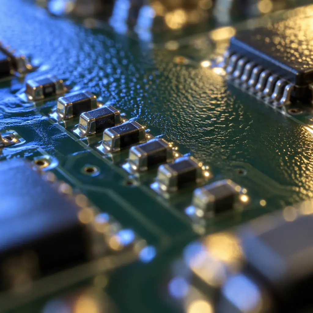
Six conformal coating defects, the process parameter behind each, and the IPC-A-610 Class 2 and Class 3 accept/reject verdict. Includes PO clauses.
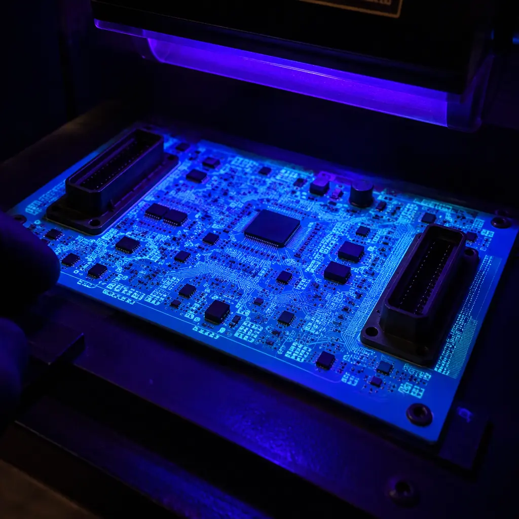
How to specify and verify conformal coating coverage with UV tracer: keep-in zones, inspection limits, the thickness correlation trap, and testable PO wording
How goods-in BOM and MPN verification catches wrong part, wrong reel and counterfeit risk before SMT: what is checked, with what equipment, and what it costs.
Upload your Gerber files and BOM. We'll respond within 24 hours with a detailed quote and free DFM review.