
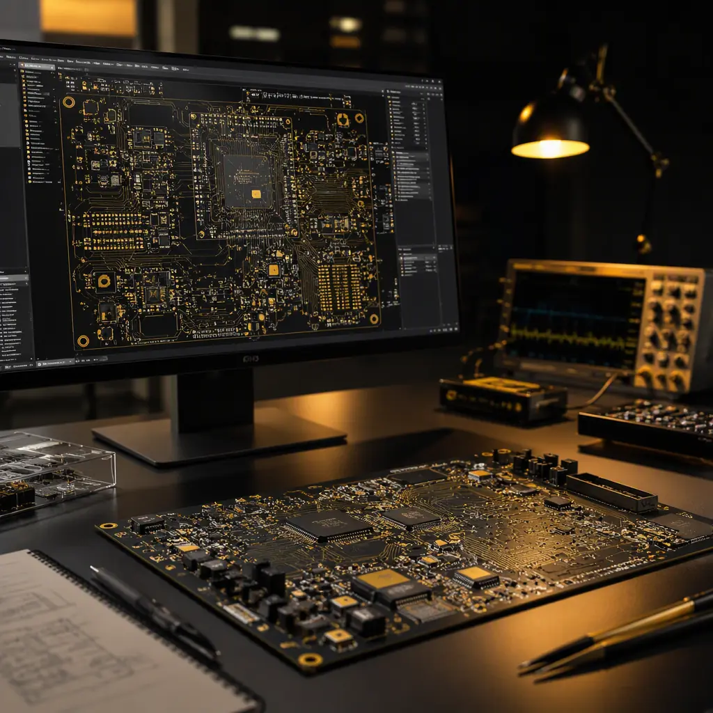
The single most expensive place to find a design problem is on a populated assembly line after three prototype rounds and a blocked production schedule. The cheapest place to find it is on a schematic and layout review before the Gerber files ever leave your desk. That is the whole idea of shift-left verification. Moving design-for-manufacturing, signal-integrity and testability checks as far upstream as possible, so the cost of a fix stays low and the cycle never stalls.
The economics are simple and they compound. A defect caught in a pre-fabrication DFM review might cost a few hours of a design engineer. The same defect caught at first-pass SMT rework can cost days and a fresh panel run. Caught in the field, it costs a recall. At Huaxing PCBA, our engineering team runs a structured shift-left review on every incoming project, laying the stackup, the impedance targets, the solder-mask and silkscreen, the stencil and the test strategy before we commit copper. It is part of how we hold a 99.2% on-time delivery rate and a 98.7% first-pass yield across 150+ active customers.
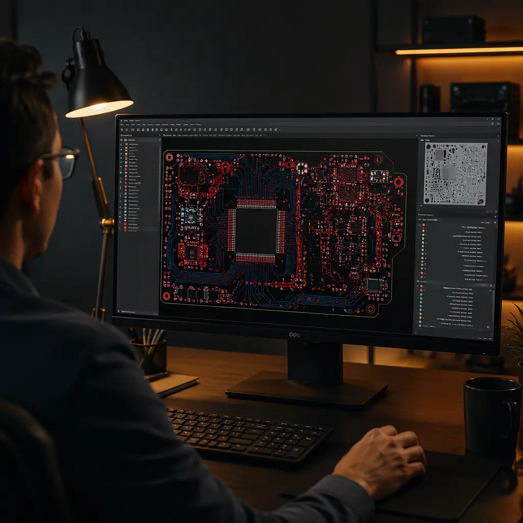
Why the Cost of a Fix Grows as It Moves Downstream
The shift-left argument rests on a well-established cost curve: the later a defect is found, the more expensive it is to correct, because each downstream stage adds rework labour, material, schedule and qualification. For a board manufacturer the curve is steepest between the design review and the first assembly pass, which is exactly where most DFM savings live.
| Stage where a defect is caught | Relative cost to fix | Typical cycle impact |
|---|---|---|
| Pre-fabrication DFM review | 1× | None, caught in hours |
| After first panel run | 5–10× | Adds a re-spin and a fabrication cycle |
| After first SMT assembly | 20–50× | Adds rework, potential yield loss |
| After field deployment | 100×+ | Recall, warranty, brand damage |
This is why the most sophisticated procurement teams ask a supplier not "can you build this" but "will you tell me what is wrong before I spend the money on a first run." The answer depends entirely on whether the supplier runs a real shift-left review or simply takes the files to the line and reports surprises after the fact.
What a Shift-Left Review Actually Checks
A shift-left verification is more than a spell check on a Gerber file. It is a structured gate that covers manufacturability, reliability and testability before any material is committed. The components below are the ones that most often bite a first run, and the ones worth asking about in a DFM service.
Stackup, layer count and impedance
Is the layer count right for the impedance and routing density? Are the impedance targets on the right layer and referencing a solid ground plane? Getting this wrong upstream forces a full re-spin. Our stackup design and layer-count selection guides cover the trade-offs.
Copper, clearance and annular ring vs your capability
Minimum line width and spacing, annular ring, via-to-trace clearance and copper balancing all affect yield and cost. A review that flags a 3 / 3 mil trace on an area that could be 6 / 6 mil is a review that just saved you money.
Solder-mask, silkscreen and paste coverage
Mask openings over pads, silkscreen clearances, component-placement conflicts and paste-layer coverage drive SMT yield. A stencil design and mask check here prevents bridging and opens. Our solder-mask types article explains the options.
Assembly process review: footprints, pitch and stencil
Are the footprints and padsizes right for the chosen process? Can the parts be placed, reflowed and inspected? Does the stencil aperture and thickness match the paste requirement? Our stencil design guide and assembly process walkthrough cover it.
Testability and access
Can the board actually be tested? Test points, probe access, ICT fixture design and boundary-scan provision are the difference between a board you can verify and one you can only visually inspect. See our testing methods guide for the ICT, flying-probe and functional-test trade-offs.
Signal integrity and design rules (for high-speed)
On high-speed or RF boards, a pre-layout and pre-fab simulation check on termination, reference planes and via returns prevents a board that only works by luck. This is where a supplier with real signal-integrity engineering earns its keep.
Key Takeaway: A shift-left review is a structured gate, not a courtesy. Stackup, copper, mask, assembly, testability and signal integrity should all be checked before fabrication, and flagged to you as findings, not surprises.
Simulation: The Part Most Suppliers Skip
Static DFM rule-checking catches geometric conflicts. Simulation catches the more expensive problem, behaviour. On high-speed, power or RF designs, a decent supplier runs simulation for the things that do not show up as a "clean error" in a rule check: impedance continuity, crosstalk, power-integrity on the supply rails, and thermal hotspots. When simulation is included, the review moves from "this layout obeys rules" to "this layout will actually work," which is the distinction that prevents a four-round NPI.
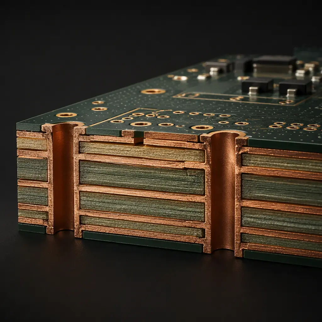
For the fundamentals that underpin a robust first pass, read our Gerber files guide and materials guide . They cover the file set and the materials that the DFM review evaluates.
The Two Rounds vs Four Rounds Economics
The clearest way to value shift-left is to contrast a well-reviewed project with a poorly-reviewed one. With a thorough pre-fab review, a typical board goes from design to a production-representative sample in two NPI rounds. Without it, three, four or more rounds are common, each adding fabrication, assembly, test and calendar time, and each one burning schedule in a product launch.
| NPI outcome | With shift-left review | Without |
|---|---|---|
| Rounds to production-ready | 2 | 3–4+ |
| Re-spin likelihood on a typical board | Low | High |
| Time-to-production sample | 2–3 weeks | 5–8 weeks |
| Rework and scrap cost | Low | Significant |
Procurement Tip: When you request a quote, ask for the DFM review as a first deliverable, before fabrication. A supplier that is confident in its process will flag issues early and document its capacity limits. A supplier that only talks price is moving the risk to your launch.

To turn the review into a repeatable process, combine it with our DFM tips for the layout checklist and the PCBA NPI process guide for the whole new-product-introduction flow, from files through first article to ramp.
At Huaxing PCBA we run 8 SMT lines, 4 DIP lines and 32-layer fabrication inside a 15,000 m² facility with 500+ staff, processing over 8 million placements per day for customers in 30+ countries. Our engineering team performs a structured shift-left DFM review on every incoming project, covering stackup, impedance, copper, mask, assembly and testability before we commit copper. We are ISO 9001, IATF 16949 and UL (E354321) certified, with a 99.2% on-time delivery and 98.7% first-pass yield. Upload your files for a quote or talk to our engineering team about a DFM review before your first run.
