

Blog
Technical articles on PCB design, manufacturing, and industry best practices. Written by our engineering team.
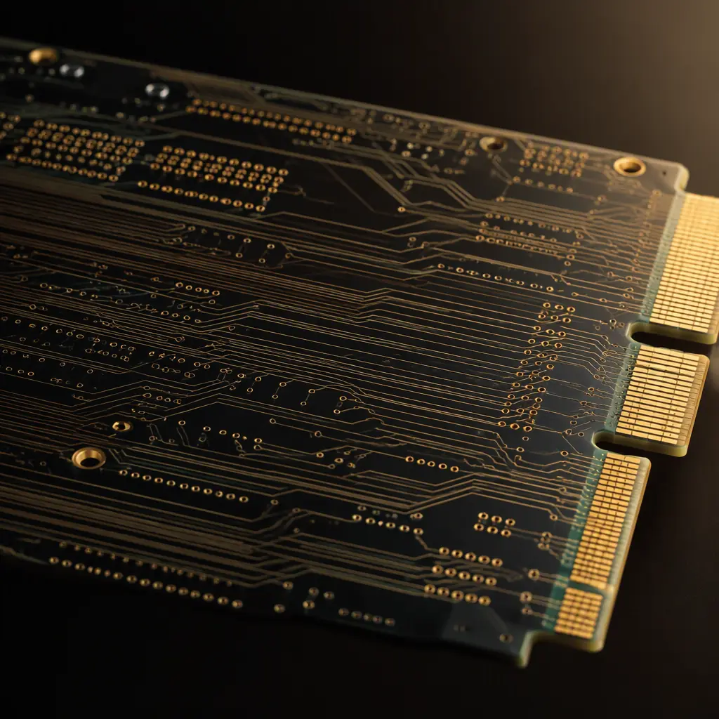
Designing a board for 112G or 224G SerDes is a channel problem, not a routing problem. Learn the insertion-loss budget, low-loss laminate selection, backdrill a
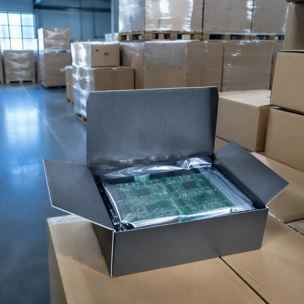
A PCB purchase order is the bridge between a quote and a build — and it is where most ambiguity creeps in. Learn what to put in a PO, how order confirmation pro
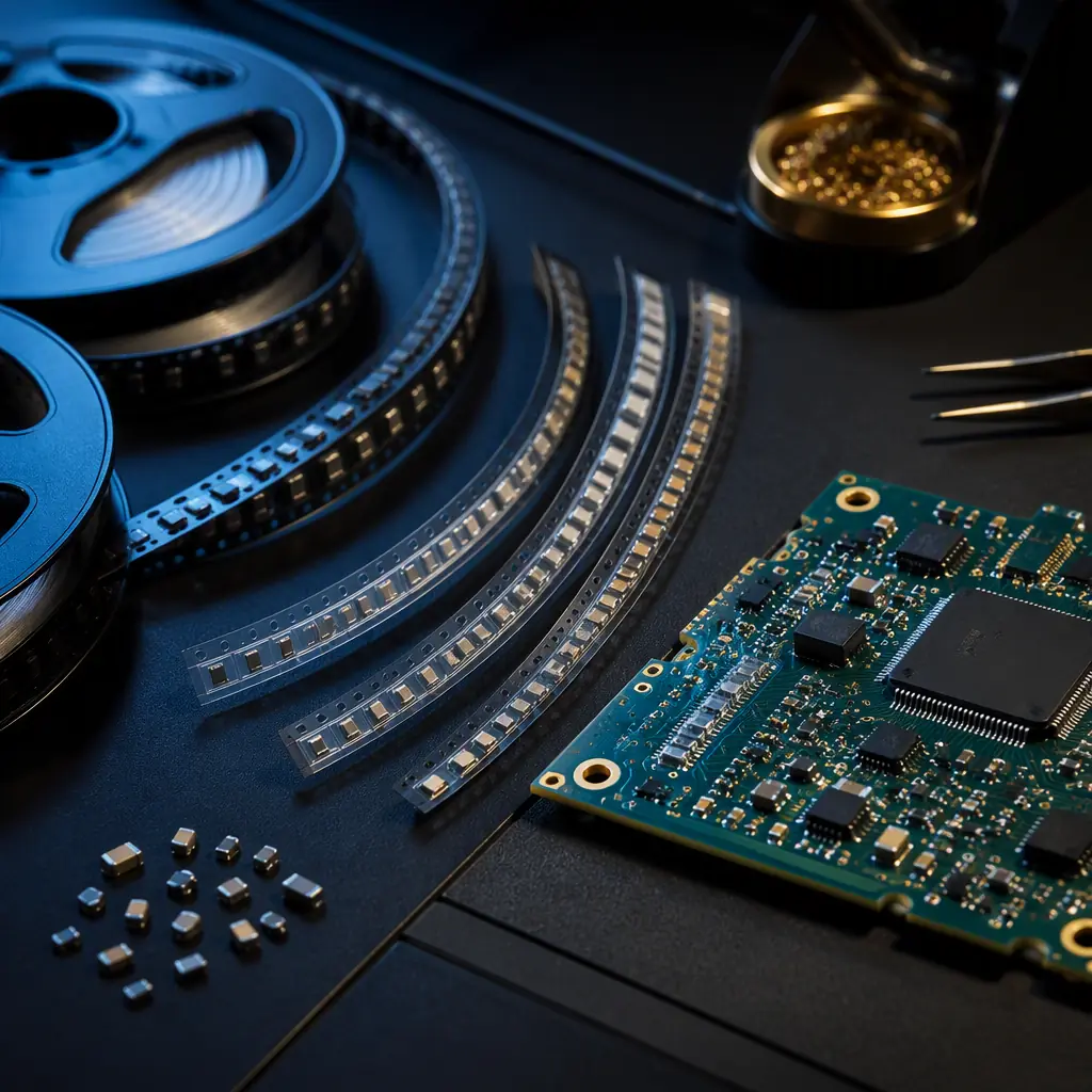
A BOM for PCB assembly is not a parts list — it is a manufacturing contract. Learn the required fields, the consignment vs turnkey difference and the 7 mistakes
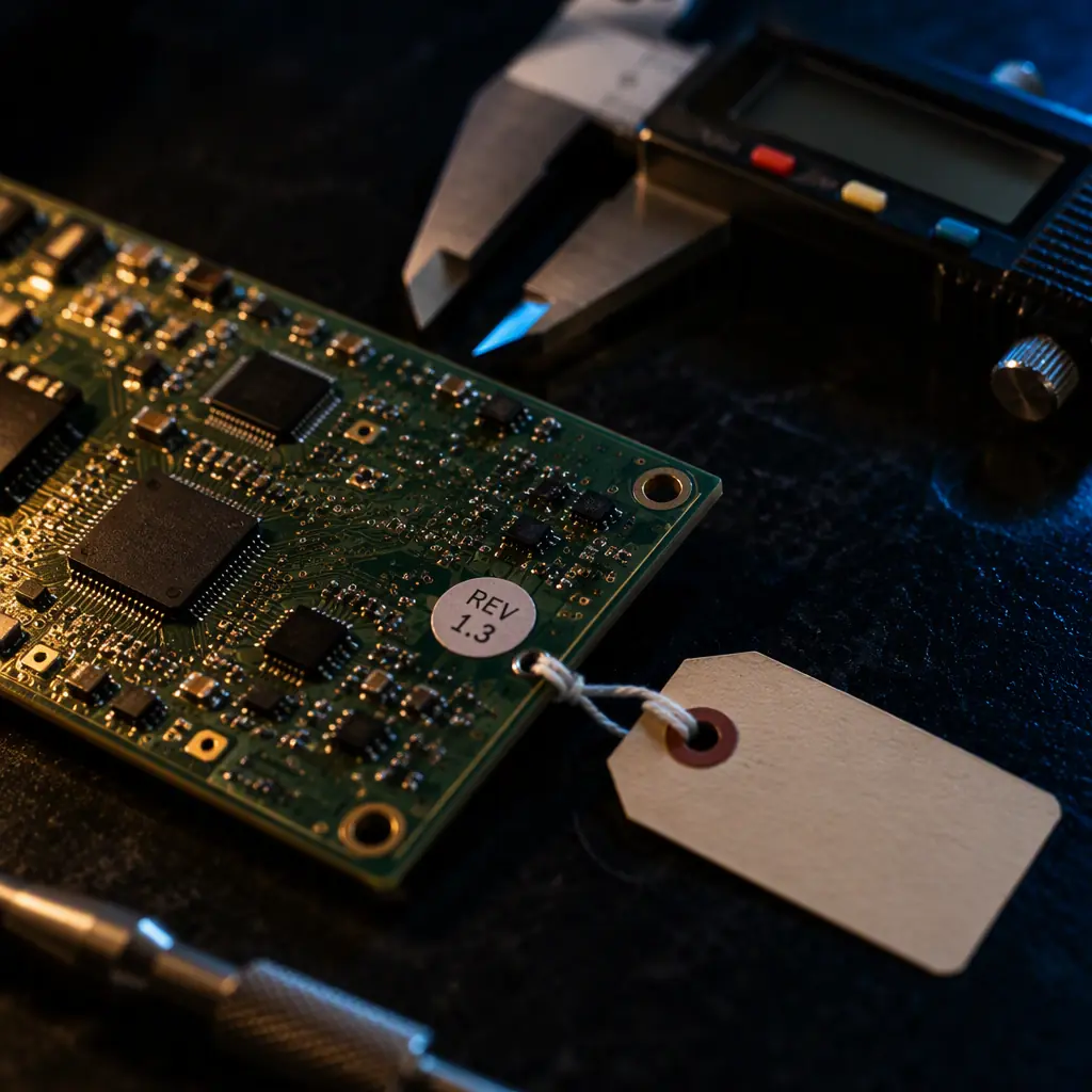
An ECO to a PCB has ripple effects far beyond the board: re-quotes, stale parts, old stencils and a scrap pile. Here is how a disciplined revision-control and e
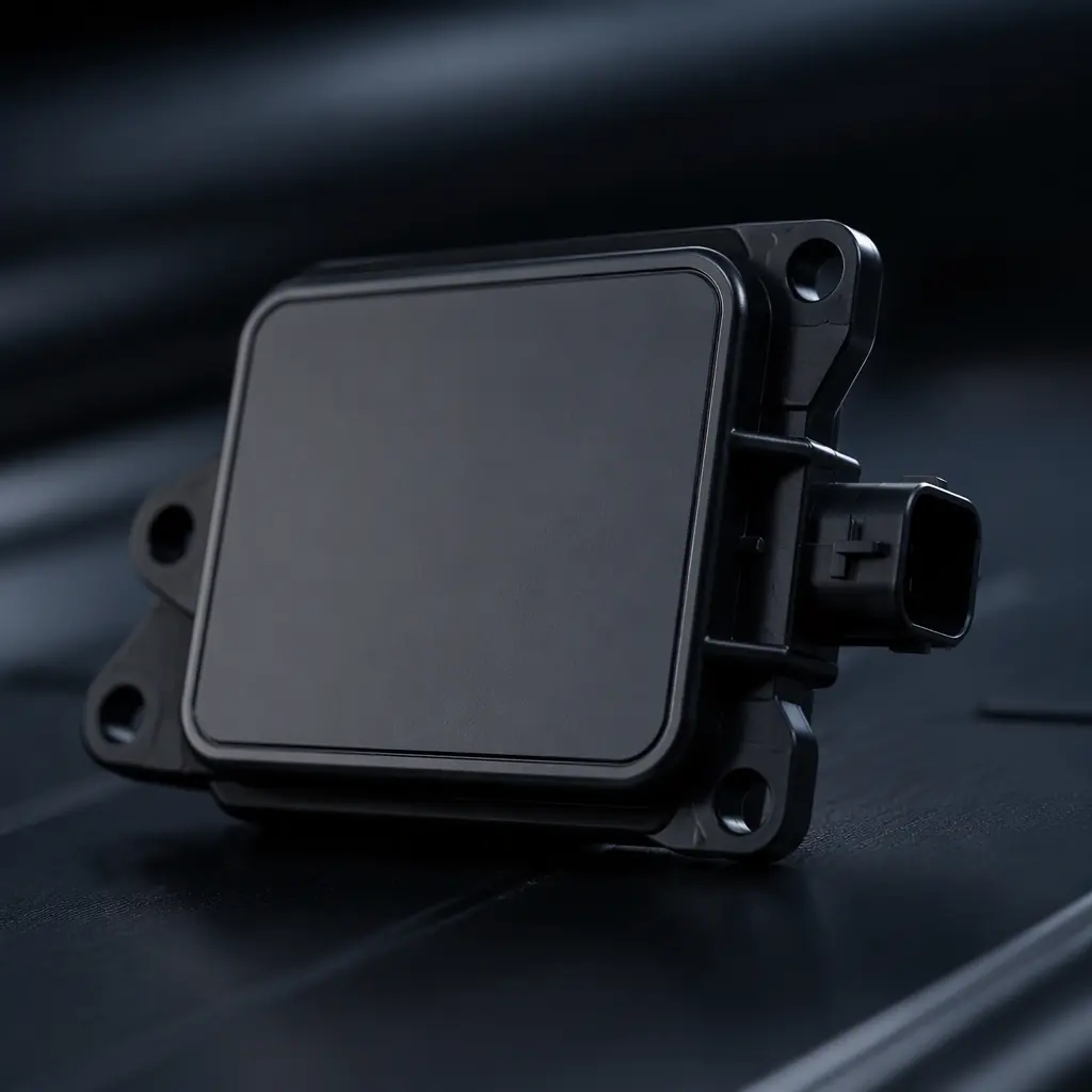
Designing a 77-81 GHz automotive radar PCB is a high-frequency discipline: low-loss RF laminate, tightly toleranced etching, MMIC and patch-antenna integration,
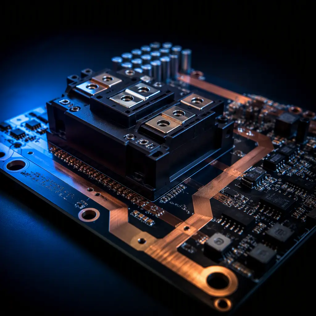
Wide-bandgap SiC and GaN switch faster than silicon, so your PCB is suddenly the bottleneck. Learn gate-drive layout, loop inductance, high dV/dt EMI, creepage

Conductive anodic filament (CAF) is a hidden PCB reliability killer that only shows up months into field use. Learn the failure mechanism, the IPC-TM-650 2.6.25

Custom PCB design and assembly for agricultural electronics and precision farming: IP67 washdown ruggedization, low-power solar operation, environmental sealing
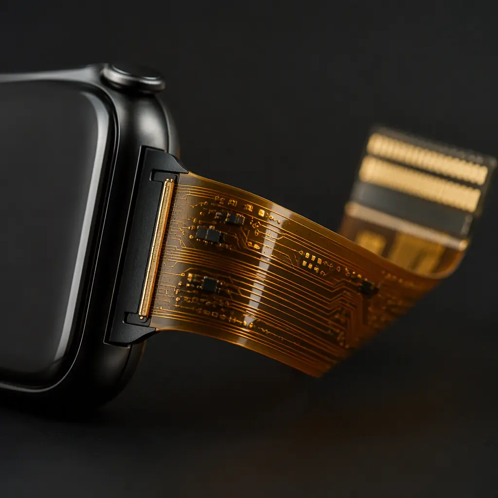
Flexible PCB design for wearables and smartwatches: bend radius limits, thin-film layer stackup, HDI microvias, IP67 sealing, low-power layout and assembly of 0

Upload your Gerber files and BOM. We'll respond within 24 hours with a detailed quote and free DFM review.