
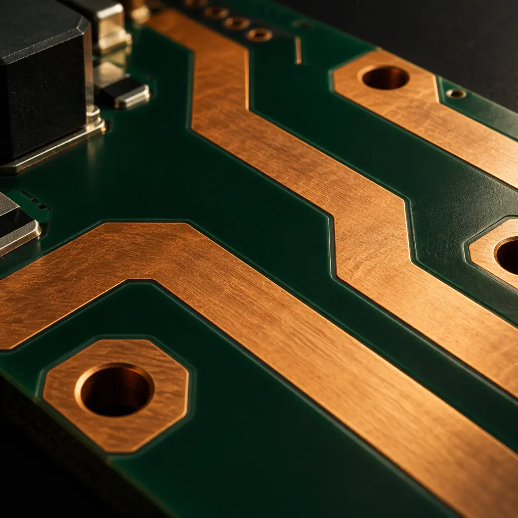
The most common high-voltage layout mistake is not a wrong component — it is spacing carried over from a low-voltage design and never revisited. A board that works perfectly at 24 V can fail an insulation review at 400 V because the copper-to-copper gaps were chosen for manufacturability, not for voltage. Creepage and clearance are the two distances that govern whether current can track across a surface or jump through air, and both are functions of the working voltage, the environment the board operates in, and the material it is made from.
These rules matter increasingly because more products now mix high and low voltage on one board. An on-board charger, a solar inverter, a portable power station and an industrial motor drive all put mains-referenced circuitry onto the same substrate as control logic. Getting the spacing right is not just a safety-formality — it decides whether the isolation holds after a few years of contamination and thermal cycling, and it is one of the few design decisions that a fabricator can check for you before the build if you ask.
This article covers the difference between creepage and clearance, the governing standards (IPC-2221 for spacing versus voltage, IEC 60664-1 for insulation coordination), how pollution degree and material group change the tables, the altitude derating that catches engineers out, and how slotting, potting and conformal coating are used to legally reduce creepage distance. For the power stages where these rules live, see our articles on EV on-board charger and DC-DC PCB, solar inverter PCB manufacturing and portable power station PCB design.
At Huaxing PCBA we fabricate high-voltage and isolation-grade boards across 8 SMT lines under IATF 16949 and ISO 9001, with minimum copper-to-edge and inner-layer clearance controlled to the drawing and verified on the coupon. Spacing is a design responsibility, but the fabrication tolerance that eats into it is ours, so we review both before committing to a build.
Creepage vs Clearance: Two Distances, Two Paths
The two terms are often used interchangeably, which is the first thing to fix. They describe different breakdown paths and are governed by different physics.
Clearance is the shortest distance through air between two conductive parts. It governs the air gap — the point at which voltage can simply arc across the space. Clearance is what protects against a transient overvoltage event, and it is why connectors on mains-referenced boards are often visibly spaced apart.
Creepage is the shortest distance along the surface of the insulating material between two conductive parts. It governs surface tracking, where contamination, condensation or a build-up of conductive residue gives current a path to crawl across the board. Creepage is usually the larger of the two and is the one that gets redesigned when a product fails in a humid environment.
Because creepage follows the surface, it is affected by the shape of the surface and by anything sitting on it. That is the key to the later sections: anything that lengthens the surface path — a slot, a raised barrier — increases effective creepage for the same physical footprint. Anything that contaminates the surface reduces it.
The Governing Standards: IPC-2221 and IEC 60664
Two standards do most of the work, and they answer slightly different questions.
IPC-2221 gives generic design requirements for printed boards, including a table of minimum conductor spacing versus voltage for different coating and environmental conditions. It is the quick-reference most PCB designers use because it speaks directly in terms of trace-to-trace spacing on a board. Its table distinguishes between bare boards, boards with conformal coating, and boards in different environments, and it scales spacing with the working voltage across the gap.
IEC 60664-1 is the insulation-coordination standard that safety agencies use for equipment. It does not just take voltage as an input — it takes the working voltage, the pollution degree of the environment, the overvoltage category of the location in the installation, and the material group of the insulator, and derives a required clearance and creepage from them. This is the standard that governs whether a product passes a safety review, and it is why a design that looks compliant to a bare IPC-2221 table can still fail certification.
The practical workflow is to design to IEC 60664 for the product's specified environment, and to use IPC-2221 as the fabrication-facing check that the trace spacing on the board satisfies it. When the two appear to disagree, the safety standard governing the product's certification wins, and the question becomes whether the review agent has accepted a particular interpretation.
Pollution Degree, Overvoltage Category and Material Group
The reason the same voltage yields different spacings for different products is these three variables. They are easy to state and easy to underestimate.
| Variable | What it captures | Effect on required spacing |
|---|---|---|
| Pollution degree (1–4) | How much conductive contamination the environment will deposit on the surface | Higher pollution degree → longer creepage required. Coating the board effectively lowers the applied pollution degree. |
| Overvoltage category (I–IV) | How much transient overvoltage the location can subject the equipment to | Higher category → greater clearance required. Mains entry is typically a higher category than downstream electronics. |
| Material group (I–IIIb, by CTI) | The comparative tracking index of the insulator — how well it resists surface tracking | Weaker material group (lower CTI) → longer creepage required. Standard FR-4 falls into a middle group; high-CTI laminates allow shorter creepage. |
Pollution degree. A sealed, climate-controlled industrial cabinet is a mild environment; an outdoor or dusty one is not. The pollution degree assumed for the design must match where the product actually goes, and it is routinely taken as more benign than reality. Coating the assembled board is the standard way to claim a lower effective pollution degree — but only if the coating is properly applied and covers the relevant surfaces, which brings its own qualifiability requirements.
Material group and CTI. The comparative tracking index measures how a material resists forming a conductive carbonised track when contamination and voltage combine. Higher CTI means better resistance and, in the IEC tables, permits shorter creepage for the same voltage. Standard FR-4 typically sits in a mid material group. Selecting a higher-CTI laminate is one of the legitimate levers for fitting a high-voltage design into a constrained space, but it changes the material cost and must be specified, not assumed. Our guide to manufacturing tolerances covers how fabrication variation interacts with these spacing choices.
Overvoltage category. The same nominal voltage can require different clearance depending on where in the installation the equipment sits. Equipment fed directly from a mains distribution point sees larger transients than equipment behind an isolation transformer. Mapping your product to the correct category is part of defining the design inputs, not an afterthought.
Altitude Derating: The Trap That Only Shows Up in the Field
Clearance is a distance through air, and the dielectric strength of air falls as pressure falls. At high altitude the air is thinner, so a gap that reliably holds off a voltage at sea level can flash over at 2,000 metres. This is why IEC 60664 includes an altitude correction factor that increases the required clearance above 2,000 m, and why a design validated at a coastal lab can fail on a mountain installation.
The trap is that altitude is rarely on a design's list of stated requirements. If your product ships to customers in high-altitude regions — or to any market where the end use is not controlled — the altitude assumption needs to be explicit in the design inputs. A 400 V gap comfortably designed at sea level may need noticeably more clearance at 3,000 m, and that clearance is measured through air, so it cannot be recovered by slotting or coating. Clearance must be physically present.

Slotting, Potting and Coating to Reduce Creepage
Creepage follows the surface, so shortening the required distance is a geometry problem. Three techniques are used, and each has conditions attached.
Slotting
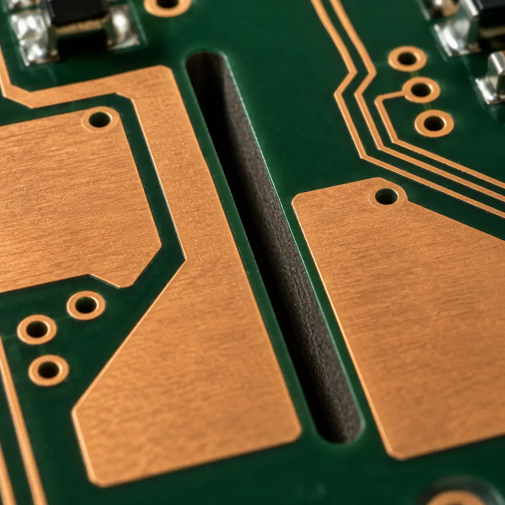
A milled slot through the board interrupts the surface path, so current can no longer creep straight across. Because creepage is measured along the surface, routing around a slot lengthens the path for the same board area. The slot must be wide enough and clean enough to actually break the track, and it does nothing for clearance — the air gap through the slot still has to satisfy the clearance requirement.
Potting and encapsulation
Filling a region with a solid encapsulant replaces air and exposed surface with a dielectric, changing both creepage and clearance behaviour. It is a common approach for ruggedised and outdoor products, but it must be a qualified process with controlled void-free fill, or the benefit is not real.
Conformal coating
Coating the assembled board seals the surface against contamination and is the standard route to claiming a lower effective pollution degree, which in turn reduces the required creepage. The catch is coverage and quality: coating that misses a surface, or lifts after thermal cycling, does not deliver the credit claimed. If you rely on coating for spacing credit, it becomes a controlled, inspected process, not a cosmetic finish.
All three techniques buy creepage. None of them buys clearance, which is a physical air path. If your clearance is short, no amount of coating will fix it — the gap has to be there.
Specification Traps and the Fabrication Tolerance
Even a correctly calculated spacing can be lost between design and delivered board. The values to watch are the ones where the calculation is done on nominal geometry but the board arrives with tolerance applied.
Minimum copper-to-edge. The distance from a conductor to the board edge is set by routing tolerance and the risk of exposed copper at the edge. High-voltage designs often need more copper-to-edge than the mechanical drawing first suggests, and the routing tolerance consumes part of it.
Inner-layer clearance. Inner layers have their own registration tolerance, so a clearance that is comfortable on an outer layer may be tighter once inner-layer registration is considered. Spacing requirements apply across layers, not just on the surface.
Drill, plating and etch variation. Holes, pads and etched gaps all carry tolerance. A creepage distance measured centre-to-centre is not the same as the copper-to-copper distance after etch and registration. When a design is close to a spacing limit, the review should be done on worst-case copper-to-copper geometry, not on nominal.
The takeaway is that high-voltage spacing should be specified with margin for the fabrication tolerance, and that the fabricator's capability data is part of the input. Ask for the achievable copper-to-edge and inner-layer registration for your build before you commit a tight design.
Summary: Four Variables, One Budget
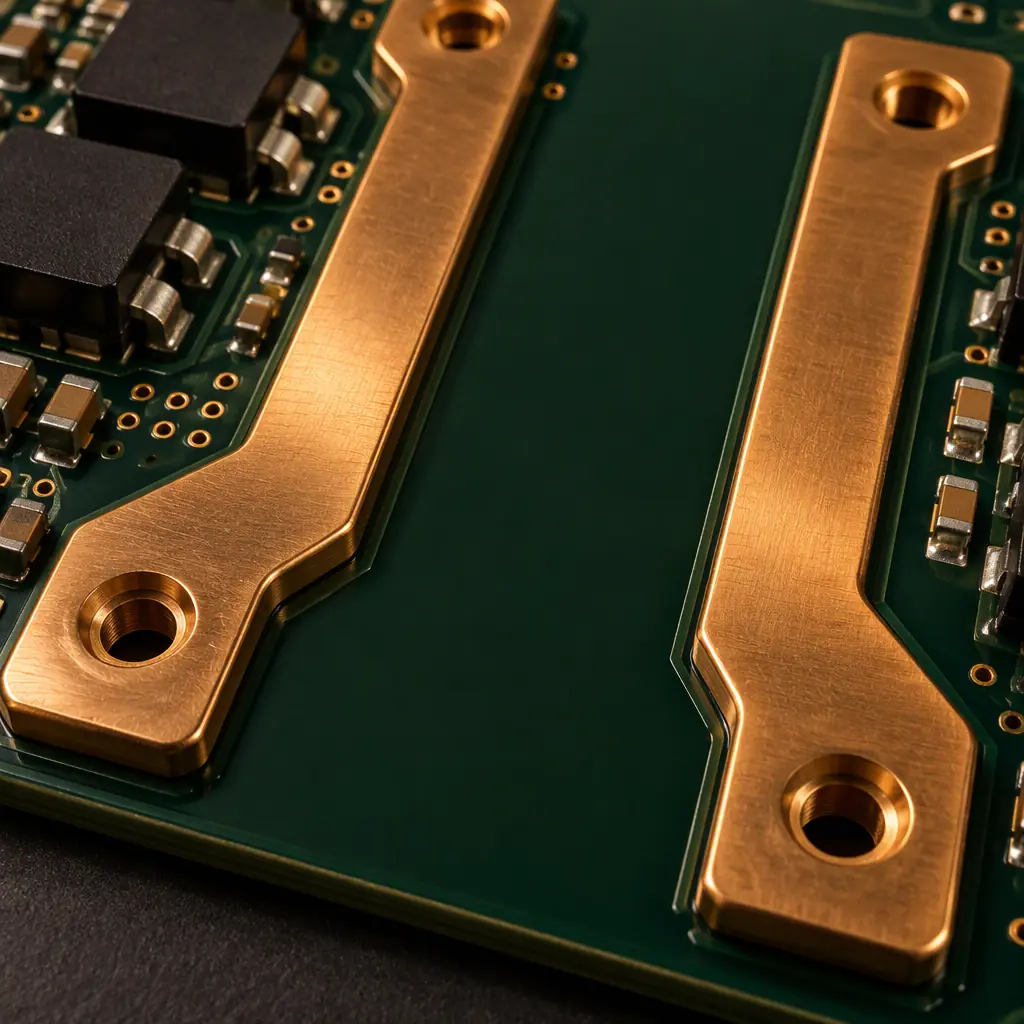
Creepage and clearance are separate distances — one along the surface, one through air — and both are functions of voltage, pollution degree, material group and altitude. IPC-2221 gives the fabrication-facing spacing check; IEC 60664-1 gives the insulation-coordination numbers a safety review uses. Slotting, potting and coating can legitimately reduce creepage, but clearance is physical and cannot be coated away, and altitude derating catches designs that were validated at sea level. Specifying all four inputs explicitly, designing to worst-case copper-to-copper geometry with fabrication margin, and confirming coverage where coating carries the spacing credit is what keeps a high-voltage design compliant from prototype through certification.
At Huaxing PCBA we fabricate high-voltage and isolation-grade boards with drawing-controlled copper-to-edge and inner-layer clearance, across 8 SMT lines under IATF 16949 and ISO 9001. If your new design mixes mains-referenced and control circuitry, send us the Gerber early and we will review the spacing against our process capability. Send your Gerber and BOM and we will return a quote with the DFM review inside 24 hours, or talk to our engineering team about a high-voltage spacing question you are working through.
