
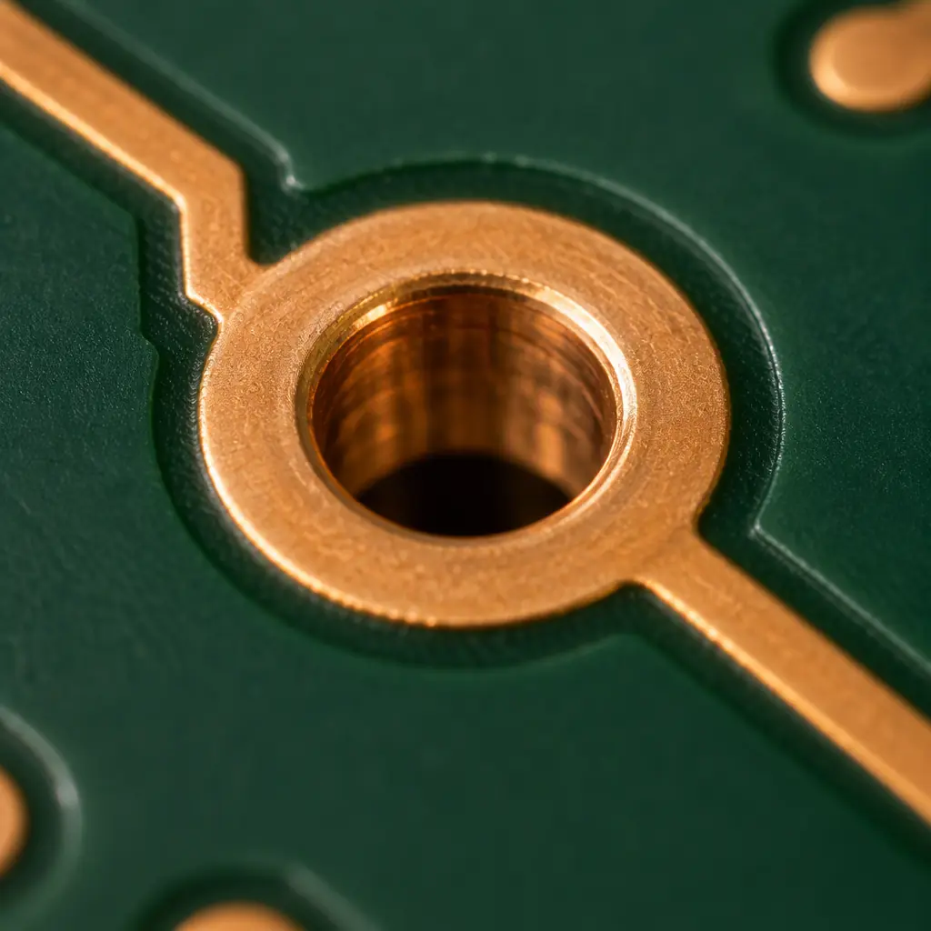
Ask most designers what their minimum annular ring is and you will get a number: 5 mil, 6 mil, whatever the last DFM report said. That number is the nominal value, and it is not what the fabricator delivers. Annular ring is the difference between the pad diameter and the finished hole diameter, and every step between design and finished board — drilling, plating, etching, layer-to-layer registration, and the dimensional movement of the laminate itself — eats into that difference. What matters for yield is not the ring you specified but the ring that survives the tolerance stack.
This matters more than it sounds. A broken annular ring means a pad that is no longer fully supported by copper around the hole. In a rigid board it can pass electrical test cold and then crack in the field as the barrel expands and contracts. In a dense HDI design with thousands of small vias, the smallest holes carry the least nominal ring and are the first to break out. Understanding the ring as a budget rather than a fixed dimension turns an abstract spec line into something you can reason about — and it tells you which parts of your design are quietly at risk before you ever commit to a build.
This article covers the definition of annular ring and how it differs on internal and external layers, the minimum ring sizes in IPC-2221 and IPC-7351 by class, how IPC-A-600 grades a breakout or tangency, the tolerance drift that turns a nominal ring into a delivered one, and why small vias fail first. For the tolerance stack this depends on, see our guide to PCB manufacturing tolerances; for the drilling side, see hole accuracy and drilling tolerance. For the land pattern that sets the pad size in the first place, see IPC-7351 land pattern density levels.
At Huaxing PCBA we specify minimum annular ring by class in the fabrication drawing and verify it in cross-section as part of first-article and ongoing process control across 8 SMT lines under IATF 16949 and ISO 9001. The check is written into the process because ring is one of the few parameters where a design that looks fine in CAD can still be marginal once the drill tolerance is added.
What Annular Ring Actually Is
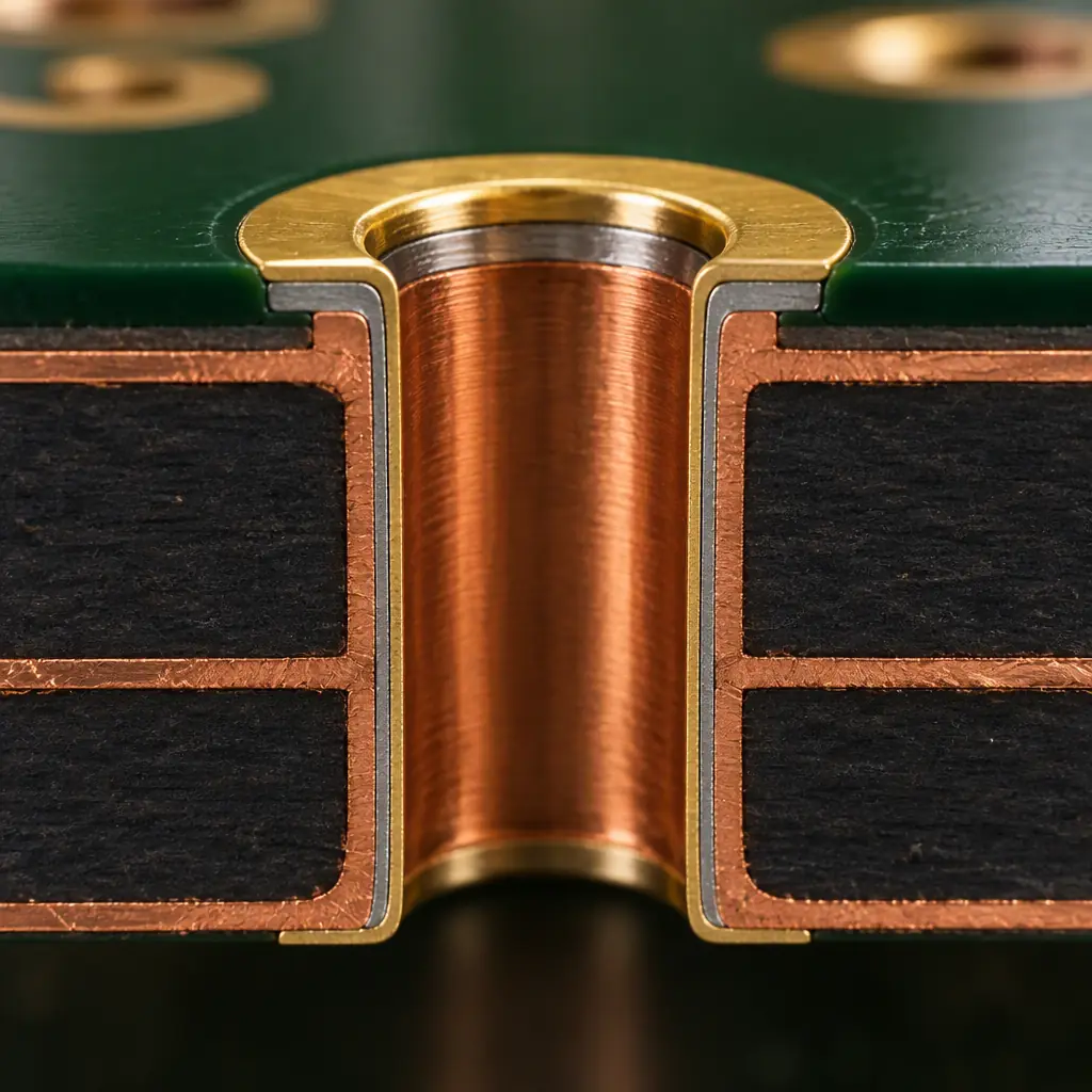
Annular ring is the width of copper that surrounds a plated hole, measured radially from the edge of the finished hole to the outer edge of the pad. If a pad is 24 mil in diameter and the finished hole is 12 mil, the annular ring is 6 mil on each side — nominal. That is the easy case. The complications start as soon as you ask which hole and which pad edge you are measuring against.
Finished hole size, not drill size. The number on your drill file is the tool diameter. After plating, the hole is smaller by roughly the plating thickness on each wall — typically around 1 mil of copper per side for standard plating, though it varies with the target wall thickness in the fabrication drawing. If you compute ring against the drill size instead of the finished hole size, you overestimate the copper margin. Use the finished hole size.
Internal versus external layers. An external pad is a single plane of copper, so its ring is measured directly. An internal pad sits between laminate layers, and the etch and registration behaviour is different — internal layers often have a larger nominal ring prescribed for the same drill because the etch tolerance and layer-to-layer registration are less forgiving. This is why the same hole can have one minimum on the outer layers and a different minimum internally.
Pad shape matters. A round pad has a uniform ring only if drilling is perfectly centred. In practice drill position varies around the nominal centre, so ring is smallest at the point where the drill wanders closest to the pad edge. Rectangular or elongated pads give more margin in one axis and less in the other. When you specify a minimum, you are really specifying the smallest radial measurement anywhere on the circumference.
Minimum Annular Ring by IPC Class
IPC-2221 sets generic design requirements, with the minimum annular ring widening as the reliability class rises. IPC-7351 handles land pattern geometry for the components themselves, and the two interact: the land pattern defines the pad, and the design rules define how much of that pad must remain after drilling. The short version of the external-layer minimums by class is this:
| Class | Typical minimum external ring | Where it applies |
|---|---|---|
| Class 1 — General Electronic Products | ~2 mil (0.05 mm) | Consumer, non-critical, cosmetic defects tolerated |
| Class 2 — Dedicated Service | ~2 mil minimum, 5 mil preferred | Industrial, most commercial; extended life requirement |
| Class 3 — High Reliability | ~2 mil minimum with no breakout, tightened by drawing | Medical, automotive safety, aerospace, defense |
Two things about this table are easy to misread. First, the absolute minimum in the standard is not the recommend-for-design value. Designing to the floor leaves nothing for process variation, and a shop running at the floor on a good day will break rings out on a bad one. Industrial practice is to design well above the minimum — the commonly cited 5 mil external and 1 mil internal floors are baseline design targets, not aspirational ones. Second, internal-layer minimums in the standard are typically stated separately and are often larger than the external figure because internal registration is less forgiving.
What "no breakout" means for Class 3. Class 3 does not merely reduce the allowed ring — it changes the acceptability of breakout entirely. Where Class 2 may permit a breakout that does not exceed a stated arc, Class 3 generally does not permit the pad to be reduced in a way that could affect the connection. If your product is medical or automotive, the class statement in your fabrication drawing is doing real work, and it should match the class your assembler will inspect to.
Breakout, Tangency and How IPC-A-600 Grades Them
IPC-A-600 covers the acceptability of printed boards, and it draws a specific distinction between three conditions around a hole. Understanding the terminology prevents arguments at incoming inspection.
Full annular ring. Copper surrounds the hole completely, and the remaining ring meets the design minimum. This is the good state.
Tangency. The drill has wandered far enough that the pad edge is tangent to the hole wall — the copper is still continuous around the hole, but at one point it is essentially zero-width. Tangency is a warning condition. It often passes a cold electrical test and fails later, because the barrel-to-pad connection now depends on a knife-edge of copper that thermal cycling will fatigue.
Breakout. The hole has broken through the pad edge, so the copper no longer forms a closed ring. Whether this is acceptable depends on class, the layer, and how much of the circumference is affected. Class 2 may permit a defined degree of breakout; Class 3 generally will not.
The practical takeaway for a buyer is that tangency and minor breakout are exactly the defects a visual check misses and a cross-section finds. If your product is high-reliability, the verification method matters as much as the acceptance criterion — a pad that looks connected to the eye can be a knife-edge in section. Our guide to IPC-A-600 acceptance criteria covers the visual side; cross-section is what resolves the borderline cases.
The Drift Budget: Why Nominal Ring Is Not Delivered Ring
This is the part that turns a comfortable-looking design into a marginal one. The ring you specify is consumed by several independent tolerance contributions, and they add up:
Drill position tolerance
The drill does not land exactly at nominal centre; it has a position tolerance, and the finished hole is also typically slightly larger than the drill from plating and wall quality. Both move the hole edge relative to the pad.
Etch tolerance
The pad itself is etched, and etch moves the pad edge inward or outward. On fine-feature layers, a few tenths of a mil of etch variation is normal and directly reduces the remaining ring.
Layer-to-layer registration
Inner layers are registered to each other and to the drill. Registration error shifts the pad relative to the hole, eating ring on one side even when the drill itself is well centred. This is usually the largest single contributor on multilayer builds.
Material movement
FR-4 and other laminates move during lamination and after reflow. That movement is not perfectly uniform, so it can shift the pad relative to the hole in a way that varies across the panel. High-glass-transition and high-filler materials behave differently, which is why the same design can be comfortable on one laminate and tight on another.
Stack these and a nominal 6 mil ring on a dense multilayer board can easily deliver 3 mil in the worst corner. That is not a defect — it is the normal consequence of designing to nominal and ignoring the budget. The fix is to size the pad with the budget in mind: when you know the registration and drill tolerances you will be quoted, you can decide whether your minimum feature really has the margin you assumed.

Why the Smallest Vias Break Out First
The instinct is that a small hole is easier to give a healthy ring because the pad can stay small. The opposite is true in practice. Three effects compound as hole size shrinks.
Fixed tolerances, smaller features. Drill position tolerance and registration error are not proportional to feature size — a 2 mil registration error is the same absolute number whether your hole is 8 mil or 20 mil. On a small pad that fixed error is a larger fraction of the available ring, so the same processing capability produces a proportionally worse result on small features.
Drill breakage and deflection. Smaller drills are more fragile and deflect more under load, which pushes position error up exactly where you can least afford it. A worn bit adds position drift on top, which is why ring integrity and drill bit life and hit count are connected — bit wear shows up in the delivered board as hole position drift.
Aspect ratio pressure. As holes get smaller without getting shallower, aspect ratio rises and plating uniformity worsens, which affects wall thickness and therefore the finished hole size used to compute the ring. Our article on PCB via aspect ratio limits covers where this becomes the binding constraint.
The commercial consequence is that via-dense designs are the ones where ring specification deserves the most attention, not the least. If your design has thousands of small vias, the marginal ones are statistically likely to be somewhere, and the question is whether they break out comfortably within your class limit or land right at tangency.
Specifying and Verifying Annular Ring on the RFQ
Ring is easy to leave implicit and expensive to get wrong, so make it explicit in the fabrication drawing and confirm how it will be verified. The checklist below is the minimum a serious quote will be able to answer against:
State the minimum annular ring by layer and class
Separate figures for external and internal layers, tied to the IPC class of the product. Do not leave it as "standard" — the shop's standard may be looser than your product needs.
Confirm the pad sizing convention
Make sure the land pattern you use gives enough pad for the drill and the registration tolerance you will be quoted. If the design is tight, ask the fab to review pad-to-drill ratios before the build, not after.
Agree the breakout policy in writing
For Class 3, state no breakout. For Class 2, state the permitted arc if you permit any. The acceptance criterion should match the class your assembler inspects to.
Ask how ring is verified
AOI cannot see ring under a soldermask-covered via reliably. Cross-section on a coupon is the method that actually resolves tangency and marginal ring. Ask whether sectioning is part of the first-article and ongoing control for your build.
Summary: A Budget, Not a Line Item
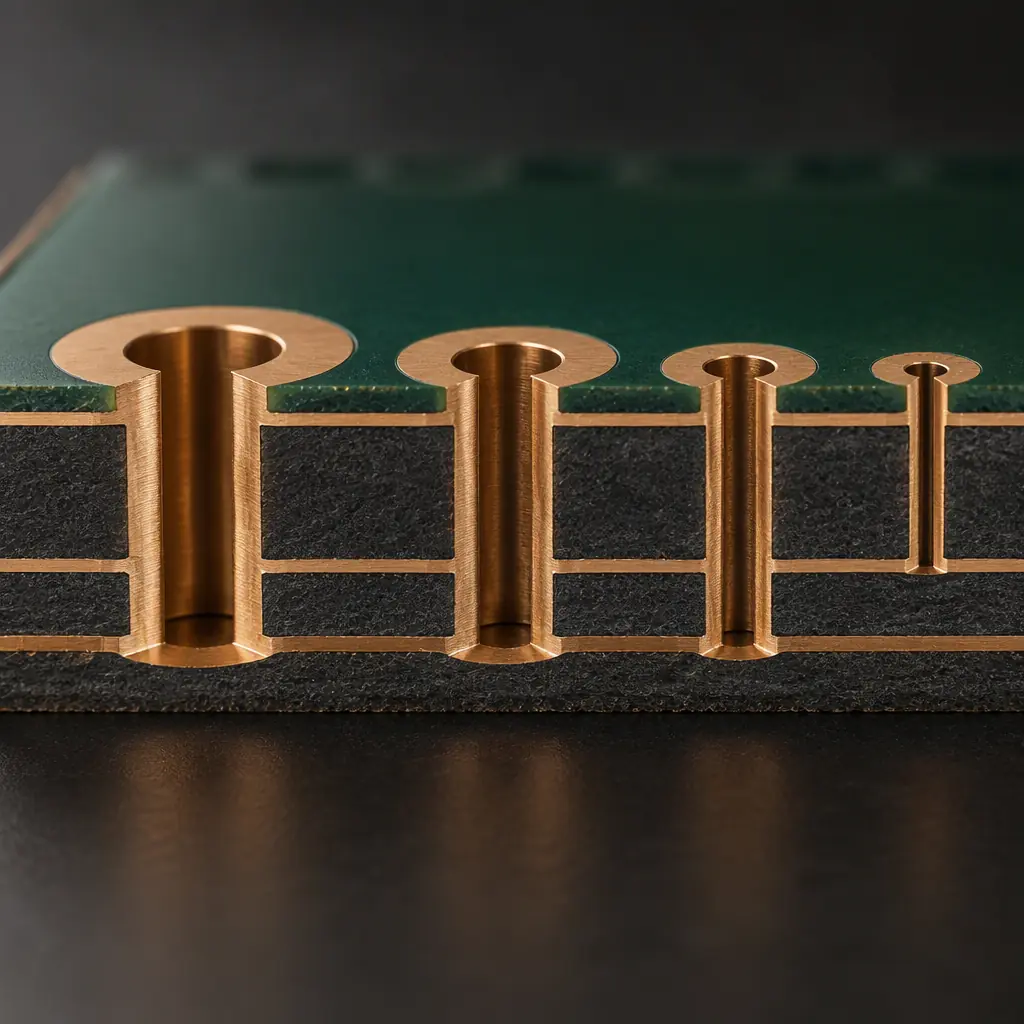
Annular ring is the difference between pad and finished hole, but what you get is that difference minus drill, etch, registration and material movement. The standards give a floor by class; good design sits well above it and sizes the pad against the tolerance stack rather than the nominal dimension. Breakout and tangency are the failure modes, IPC-A-600 grades them, and the smallest vias carry the least margin and are the ones a careful buyer worries about. Specifying ring explicitly, by layer and class, and confirming it in cross-section is a small amount of work that removes a whole class of field failures before the first build.
At Huaxing PCBA we specify minimum annular ring by class in the fabrication drawing and verify it by cross-section as part of process control across 8 SMT lines under IATF 16949 and ISO 9001. If your design is via-dense or your rings are running tight, send us the Gerber early and we will review pad-to-drill ratios before the build. Send your Gerber and BOM and we will return a quote with the DFM review inside 24 hours, or talk to our engineering team about a ring or breakout question you are working through.
