
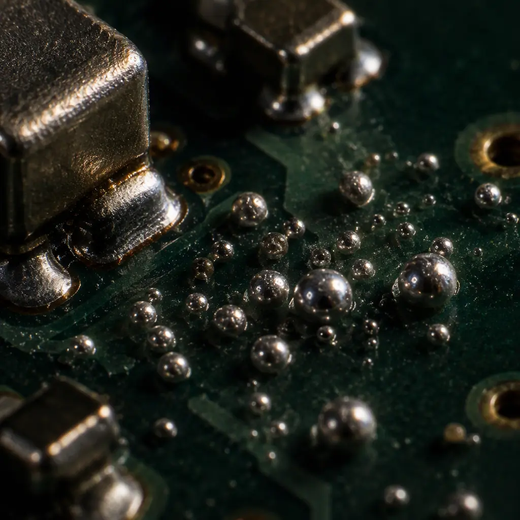
Solder balling is the presence of discrete, roughly spherical solder particles on the finished assembly, sitting on the mask, next to a joint, or trapped under a component. Beading is the related defect where the spheres form close to a specific joint or component edge. Both are visible on the board, both vary from a harmless cosmetic mark to a genuine escape risk, and both are routinely attacked in the wrong order — engineers change the paste before checking the print, or adjust the profile before checking the paste, and the defect persists.
For a buyer, the practical question is not "what causes solder balling" in the abstract, but two sharper ones: when does it matter enough to reject a lot, and is the supplier's fix addressing the real cause. This guide answers both, in an order a process engineer can actually run and a buyer can actually audit.
It belongs to the reflow defect and process-control part of this site's SMT series, alongside our guides to solder paste printing defects, solder joint defects and stencil aperture design. Balling sits at the intersection of all three.
At Huaxing PCBA we control solder balling across 8 SMT lines under IATF 16949 and ISO 9001, tracking it as a defect category against the paste parameters, stencil condition and profile window that drive it, rather than as a cosmetic issue to be touched up.
Types: Balling, Beading, Spatter and Mid-Chip Balls
The terms are related but not identical, and distinguishing them matters because each has a slightly different dominant cause.
Solder balling. Discrete solder spheres scattered on the board surface, typically where they landed after being ejected during reflow. They range from a few tens of microns to a few hundred microns. Their location is often random and away from joints.
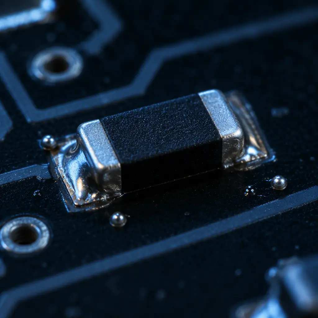
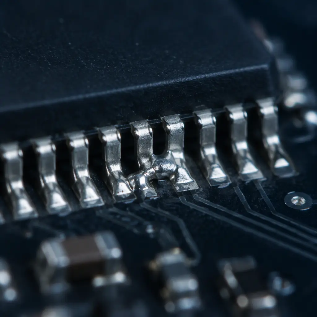
Solder beading. Spheres concentrated at the edge of a specific component or joint — most classically at the sides of a chip component or the end of a gull-wing lead. Beading points strongly to paste that was displaced when the component was placed, or to paste slump and ejection from under the part during reflow.
Solder spatter. Finer particles driven off joints during rapid heating, especially when flux volatiles escape violently. Spatter correlates with ramp rate and with paste moisture or flux chemistry rather than with placement.
Mid-chip solder balls. A specific version of beading where spheres form directly under the middle of a chip component, classically on chip resistors and capacitors. It is associated with paste deposited under the body — from stencil over-aperture, paste slump, or component standoff — and it is one of the defect types called out explicitly in assembly acceptance practice.
Key Takeaway: Where the spheres are tells you what to suspect. Scattered across the board points to paste or ramp; concentrated at a component edge or under it points to paste displacement at placement or over-aperture from the stencil.
Root Causes: Paste, Stencil and Profile
Nearly all solder balling traces to one or a combination of three sources. Working through them in a fixed order is faster than jumping to the most convenient one.
Paste. The paste is the source of the solder that forms the balls, so the paste's condition and chemistry are always in scope. Paste that has absorbed moisture forms balls more readily, because the trapped water flashes to steam during reflow and ejects solder. Paste used past its working life, or paste that was stored or warmed incorrectly, behaves the same way — the J-STD-005 storage and handling requirements exist precisely to prevent this. Paste with excessive slump collapses after printing and can deposit solder across the mask, which then reflows into balls. And paste quantity above the correct volume leaves excess solder that has nowhere to go but into spheres.
Stencil and print. The printed paste deposit is where volume and placement are set. An over-sized aperture, or a poorly matched area ratio, deposits more paste than the joint needs and pushes paste onto the mask around the pad. A stencil with inadequate tension, a sagging web, or paste smeared under the stencil between strokes leaves residue that becomes balls. Print alignment off-centre drives paste under the component body. The mechanics of aperture design and paste release — area ratio and the release behaviour that governs them — are the subject of the stencil aperture and paste release guide, and they are the most common hidden cause of beading.
Reflow profile. A preheat or ramp that is too aggressive boils off flux volatiles and moisture too fast, ejecting solder as spatter and balls. A profile with insufficient soak time leaves volatiles unexpelled before the solder melts, so they escape at peak and carry solder with them. Conversely, an over-long soak that fully dries the paste can leave dry residue that also balls. The profile's interaction with the defect is thoroughly bound up with how the profile was built, which is the subject of our reflow profile optimization guide.
The Ordered Fix Path: What to Check First
Because the three sources produce overlapping symptoms, the efficient approach is a fixed sequence that rules out the cheapest and most common causes first. This is the order to run.
Step 1 — Check the paste's age and handling. Confirm the paste is within its working life, was warmed correctly, and has not been left open or on the stencil past its allowed time. This is free and is the single most common fix. If the paste is past life or mishandled, correct that before touching the process. Paste specifications such as J-STD-005 define the characteristics the paste should hold in service.
Step 2 — Inspect the print. Look at the paste deposit before reflow: volume, alignment, spread onto the mask, and any smearing. If paste is on the mask next to the pad, the stencil or the print is the cause, and no profile change will fix it. Check the stencil for contamination, stretched webs and under-stencil residue.
Step 3 — Verify the paste volume against the aperture. If the deposit is heavy, the aperture may be over-sized or the area ratio too low for clean release. Review the aperture against the pad and the recommended paste volume for the joint.
Step 4 — Only now, review the profile. If paste and print are clean, examine the ramp and soak. A too-fast ramp with evidence of spatter, or a short soak with volatiles escaping at melt, points to the profile. Adjust the soak or the ramp rate within the process window and re-verify.
Step 5 — Cross-check the components and standoff. For mid-chip balls specifically, confirm the component standoff and the paste deposit under the body. Paste that stays under a chip body reflows into a ball regardless of the profile.
Running the sequence in this order avoids the classic waste of a full profile re-qualification when a two-minute paste-age check would have found the cause.
Acceptance Criteria: When Is It a Reject?
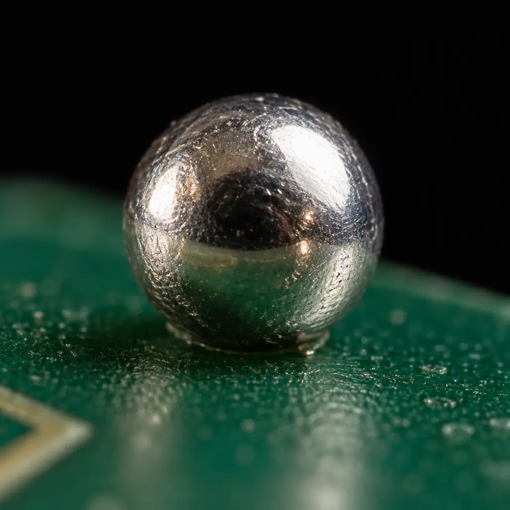
Solder balling is not automatically a defect. The assembly acceptance standard for this — IPC-A-610, the acceptability standard for electronic assemblies — treats solder balls (often called solder debris or solder balls in the standard's terminology) as a defect category with conditions, not a blanket rejection. The general logic a buyer should apply:
It is generally acceptable when: the spheres are small, are entrapped or firmly attached to the assembly, do not bridge between conductors, do not reduce electrical clearance below the required minimum, and do not sit loose where they could later migrate. Balls that are securely adhered and away from any risk of bridging are usually treated as cosmetic.
It is generally a reject when: spheres bridge two conductors or create a path between them; they reduce the electrical clearance below the specified minimum for the voltage; they are loose and could move freely — a loose ball is a latent short waiting to happen; they violate a customer, sector or safety requirement that prohibits foreign material; or they sit where an adjacent assembly, coating or conformal process could dislodge them. For high-voltage or high-reliability products, the clearance point alone often makes even attached balls unacceptable.
Those conditions are exactly why the acceptance question cannot be answered from a photo of the balls alone — it depends on size, position, attachment and the electrical context. A supplier that rejects on presence alone is over-processing; a supplier that passes tight clusters of loose balls between fine-pitch leads is under-processing.
Prevention at Design and Process Level
Preventing balling is cheaper than screening it out, and it divides cleanly between design and process.
Design and stencil. Match the aperture to the joint rather than over-sizing it; keep the area ratio within the range that releases paste cleanly; avoid placing paste apertures where they will sit under a component body; and review component land patterns against recommended patterns, as our guide to IPC-7351 land patterns describes. These decisions are made once and prevent the defect for the life of the product.
Process control. Enforce paste working-life and warm-up rules; keep the stencil clean and under-stencil wiping working; verify print volume with SPI so a heavy print is caught before reflow rather than after; and hold the profile inside its window. Each of these controls is a gate that catches a balling cause before the board is built.
Handling and environment. Humidity and handling affect paste and board moisture. Parts left out, boards exposed, and paste open to the air all raise the balling rate. The controls are the same ones that keep the rest of the process stable.
When Balling Signals a Deeper Problem
Occasionally balling that appears suddenly and across a whole run is a symptom of something larger: a paste lot that arrived out of specification, a stencil that has stretched or been damaged, a room-humidity excursion, or an oven condition that has shifted and pushed the profile out of its window. In those cases the balling is a canary — the process has drifted somewhere, and the balling is the visible edge of it.
The same logic applies on the supplier-qualification side: a supplier whose balling rate is stable and low, and who can explain the controls behind that stability, is showing process discipline. A supplier whose balling rate is variable, or who cannot connect it to paste, print and profile data, is showing the opposite. This is the same data discipline our guides to SPC and Cpk and quality metrics and DPPM describe on the statistical side.
Summary: Identify, Then Fix in Order
Solder balling and beading are visible, common, and frequently attacked in the wrong order. The first step is to identify the type — scattered balls, edge beading, spatter or mid-chip balls — and let the location point to the likely source. The second is to run the fix path in sequence: paste condition, print quality, paste volume, then profile, then component standoff. The third is to judge the result against real acceptance criteria, not against presence: attached, small, non-bridging balls away from fine-pitch conductors are usually cosmetic; loose or bridging balls, or balls that cut into required clearance, are a defect. A supplier who controls balling at the paste, print and profile stage will always be cheaper than one who screens it out at visual inspection.
At Huaxing PCBA we manage solder balling as a controlled defect category across 8 SMT lines under IATF 16949 and ISO 9001, with SPI-verified print volume, documented paste handling and profiled reflow behind it. If you are seeing balling on incoming assemblies and want to know whether it is acceptable or which control has slipped, send us the board and the defect photos. Request a quote and DFM review and we will return it inside 24 hours, or talk to our quality engineering team about a balling problem you are working through.
