
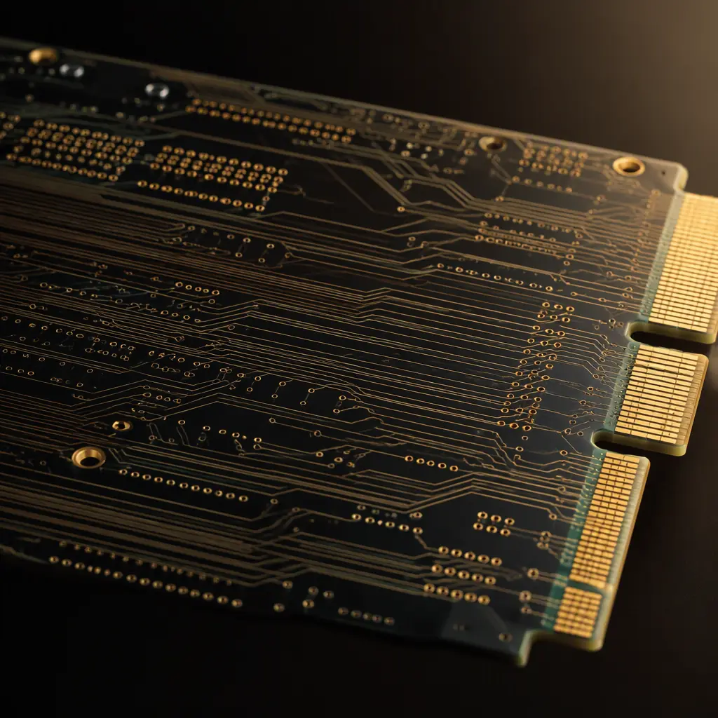
Ask most engineers what changed when SerDes went from 56G to 112G and you will get a version of the same answer: not much, just faster. The reality is the opposite. At 53.125 GBd (112G PAM4) the Nyquist frequency lands at about 26.6 GHz; at 224G, 106.25 GBd, it nearly doubles to 53.1 GHz. Once your fundamental crosses the tens of gigahertz, a trace stops being a wire and becomes a transmission line whose behaviour is governed by the whole physical channel around it.
This is precisely why a board that worked at 56G will fall apart at 112G without a single net being re-routed. The copper, the laminate, the via and the connector all have frequency-dependent loss, and a design office that buys bare boards but has never owned a channel budget usually finds this out only after a board returns and the eye opens shut. At Huaxing PCBA we fabricate backplane and switch boards to the 32-layer range with controlled impedance held to ±5%, and the difference between a good and a useless high-speed board is almost always visible on a VNA long before it is visible to the eye.
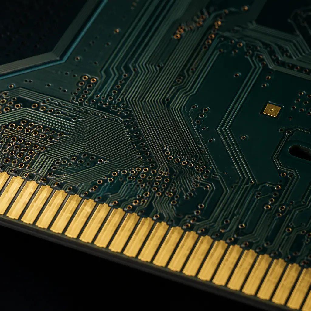
Where 112G And 224G Break From The Boards You Already Build
If your only experience of high-speed routing is a USB 3.2 or a simple PCIe lane, the jump to 112G is not a linear increment, it is a step change in how you budget the signal. Three things dominate:
Insertion loss becomes a hard number, not a nice-to-have
At 112G the channel insertion-loss budget is typically on the order of -9 to -13 dB at the Nyquist frequency once you add trace loss, via loss, connector and the BGA package. There is no crosshair on the design rule checker that warns you when you exhaust it; you have to compute it before you lay out. Our crosstalk analysis guide and signal-integrity basics cover the measurement side.
Standard FR-4 exits the conversation
Ordinary FR-4 (Dk roughly 4.2–4.5, lossy) has an insertion loss that makes it unusable once you cross roughly 25–28 GHz, and 224G doubles that. You need a low-loss or ultra-low-loss laminate. See our PCB materials guide for the substrate properties and laminate selection for how to weigh them against cost.
Via stub is now a first-class loss element
A through via on a thick board leaves an unplated stub that rings at the exact frequencies you are sending. At 112G that stub is a resonance, not a detail. Backdrilling or blind-via construction stops it. Our backdrilling guide explains the options and the HDI any-layer approach in the HDI technology deep-dive.
The Insertion-Loss Budget Is The Design
You cannot react to a loss problem after a board is fabricated, so the budget has to be set up front. A pragmatic starter budget for a 112G channel (per OIF and common backplate practice) runs roughly:
| Channel element | Typical 112G allowance |
|---|---|
| Daughtercard / blade trace | -2 to -4 dB |
| Backplane / midplane trace | -3 to -6 dB |
| Connector assembly | -2 to -4 dB |
| BGA package / silicon | -2 to -3 dB |
The takeaway is not the exact figures (they change with reach), it is that you have to allocate them. If the on-board trace eats 10 dB you have nothing left for the connector, and the board is dead before it is built. Once the budget is set, everything folds back to it: copper foil, laminate Dk/Df, line width, cross-section and the connector you spec. The stackup design is where this becomes physical.
Choosing A Low-Loss Laminate For 112G And 224G
Laminate choice is a cost-versus-loss trade, and the right answer depends on how long the reach and how tight the budget. The table below groups the common families by where they comfortably sit.
| Material family | Dk / Df range | Practical top speed |
|---|---|---|
| Standard FR-4 | Dk 4.2–4.5 / Df 0.015–0.020 | <~28 GHz, short reach |
| Mid-loss (e.g. premium FR-4) | Dk ~4.0 / Df 0.008–0.012 | 56G typical |
| Low-loss (Megtron 6-class) | Dk ~3.4–3.6 / Df 0.003–0.005 | 112G standard |
| Ultra-low-loss (Megtron 7/8, Rogers, Astra) | Dk ~3.0–3.3 / Df 0.001–0.003 | 224G, long reach |
For a 112G backplane you will almost certainly land on a low-loss material and low-profile copper. For 224G you are choosing from a much smaller club of ultra-low-loss laminates, and the copper foil becomes as important as the resin because skin effect concentrates current in the outer few microns of the conductor at 53 GHz. Rough copper loses noticeably more than smooth copper at these frequencies. Pair the laminate decision with the copper weight selection and the impedance control rules on your drawing.
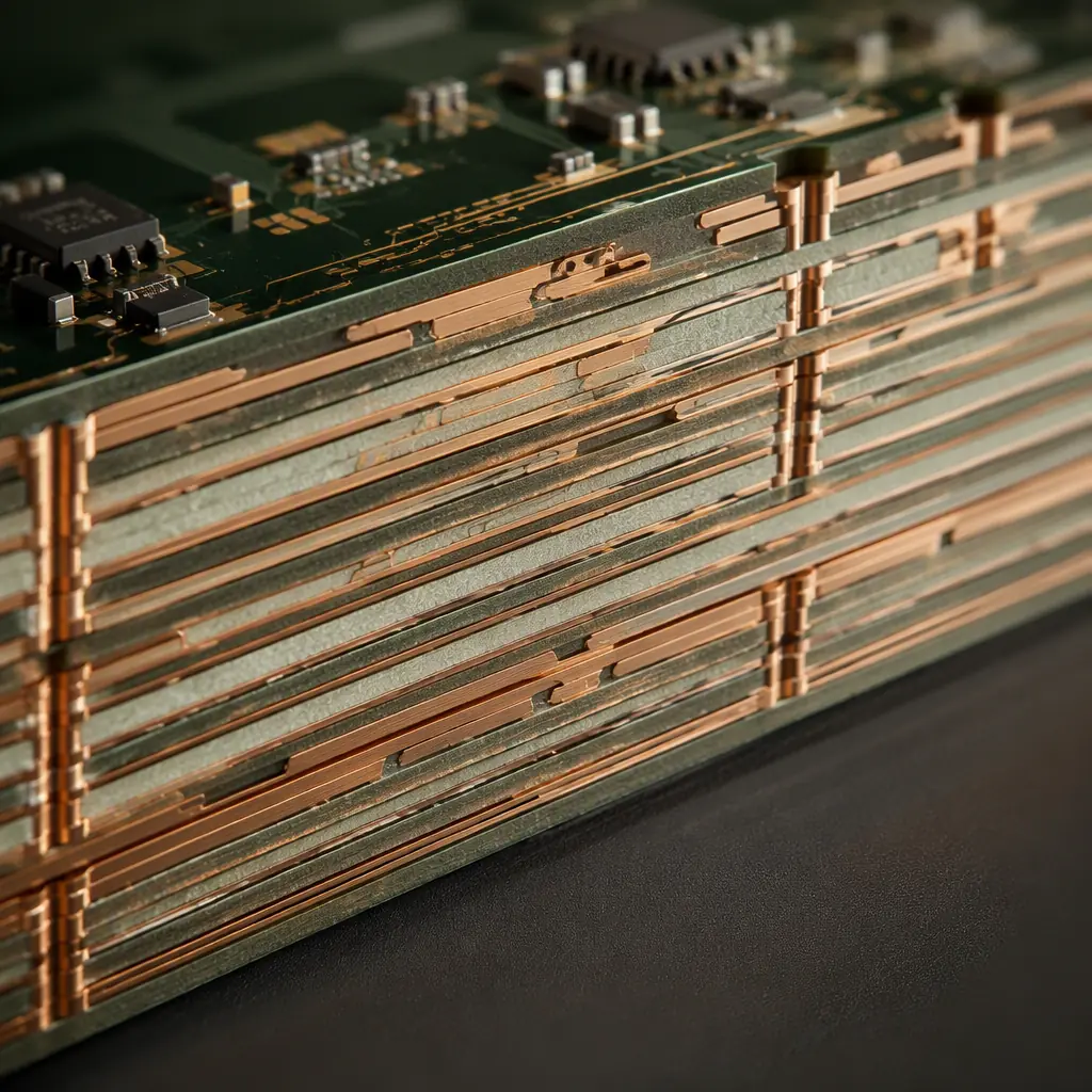
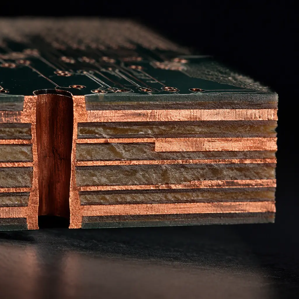
Stackup, Via Stub And Reference Planes
Once the laminate is chosen, the stackup order, the via construction and the reference planes decide whether the loss budget stays closed. A few rules of thumb hold for virtually every high-speed stack:
Put every critical layer next to a solid reference
Differential pairs need a continuous, unbroken ground plane directly above or below. A routed or slotted plane under a 53 GHz pair turns a clean channel into an antenna. Our stackup design guide shows how to order layers to keep references intact.
Control the via stub above all
Backdrilling removes the excess barrel on through vias and is the most cost-effective fix for stub resonance. Where the budget is very tight, move to blind and buried vias via HDI any-layer construction. Compare methods in our backdrilling guide.
Watch the breakout from the BGA
The nearest the pair gets to the package is usually the worst-return-loss point. Fan out symmetrically, keep the gap consistent, and move to a wide, grounded coplanar geometry. Our BGA assembly guide covers the physical side of this zone.
Crosstalk And Routing Rules For 112G And 224G
At these rates, the limit often stops being the trace you routed and starts being the neighbour you routed next to. Aggressor-to-victim energy shows up as noise on the eye you are trying to open, and it does not respect a clearance DRC flag.
Keep near-end and far-end crosstalk below roughly -40 dB where the budget allows, which in practice means generous pair-to-pair spacing, ground guards between high-speed lanes, and stripline routing for the longest reaches instead of exposed microstrip. If your signal-integrity model shows a marginal eye, revisit the routing before you spend a single dollar on material upgrades, because a spacing fix is almost always cheaper than a laminate upgrade. The crosstalk analysis piece walks through measuring it.
What To Put On The Fabrication Drawing
The best channel design collapses if it is not communicated to the fabricator precisely. For a 112G or 224G board, the fab drawing should carry these explicit callouts:
Laminate part number, grade and Dk/Df target
Name the exact material, not just "low-loss". Specify the stackup, the layer order, and the target dielectric constant with tolerance. This is the single biggest lever on the whole channel.
Impedance and tolerance
State the differential and single-ended impedance and the allowed deviation. We hold ±5% with TDR verification, state the target, not "controlled". Read more in the impedance control guide.
Copper foil requirement and surface roughness class
Call for low-profile or ultra-low-profile foil so skin-effect loss stays predictable. Plain "1 oz copper" is not a 112G spec.
Backdrill depth and the layers it clears
State the backdrill so that the remaining stub is minimal and the drill does not cut into an adjacent reference layer. Define the allowed depth tolerance.
Connectivity, test and cleanliness
Keep ionic contamination and CAF resistance in scope, and note the electrical test method, flying probe for prototypes, a dedicated fixture for volume. See our testing methods overview.
Key Takeaway: A 112G or 224G board is won or lost in the channel budget before a single trace is placed. Set the insertion-loss number up front, choose an ultra-low-loss laminate and low-profile copper to match, backdrill the stub away, guard the crosstalk, then write all of it down on the fab drawing so the fabricator can actually build what you simulated.
Summary, Engineer The Channel, Then Build It
The boards that pass validation at 112G and 224G are not the ones with the most aggressive routing, they are the ones where the engineer treated the whole channel, laminate, copper, via, connector, reference, as a single budget and then made sure the fabricator had the numbers. Material selection does more work than line width, and backdrilling does more work than adding ground pours.
At Huaxing PCBA we build multi-layer backplanes and switches up to 32 layers with any-layer HDI, line widths down to 3/3 mil, and controlled impedance held to ±5% with TDR verification. We are ISO 9001 and IATF 16949 certified, deliver to customers in 30+ countries on a 99.2% on-time basis, and can review your stackup against a target loss budget before you commit to a board. Upload your files for a quick quote or talk to a project manager about your high-speed channel.
