
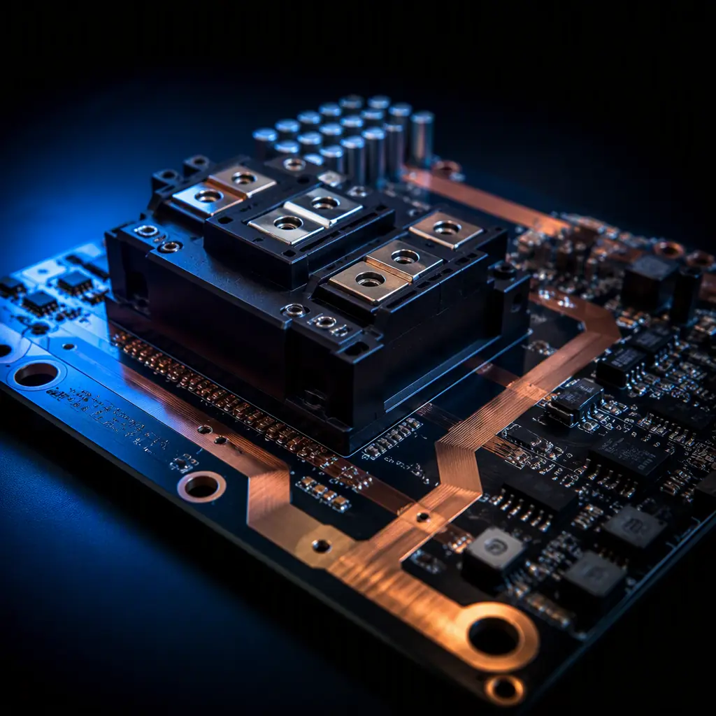
Silicon carbide and gallium nitride switches have pushed power electronics into a regime where the PCB layout, not the die, determines whether the design works. With dV/dt in the tens of volts per nanosecond and switching frequencies into the low megahertz, a trace that was fine for a silicon IGBT is now a radiating antenna, a gate loop a few millimetres too big becomes a false-trigger source, and a copper pour that cannot carry the current becomes a heat generator.
If your design uses an 800 V traction inverter, an on-board charger, a solar MPPT stage or a high-density server PSU, the rules change. Huaxing PCBA builds power-electronics boards on 8 SMT lines with 2 oz to 6 oz copper, high-Tg thermal laminates and IPC-A-610 Class 3 assembly, and we walk power designs through the parasitics and creepage requirements before quoting.
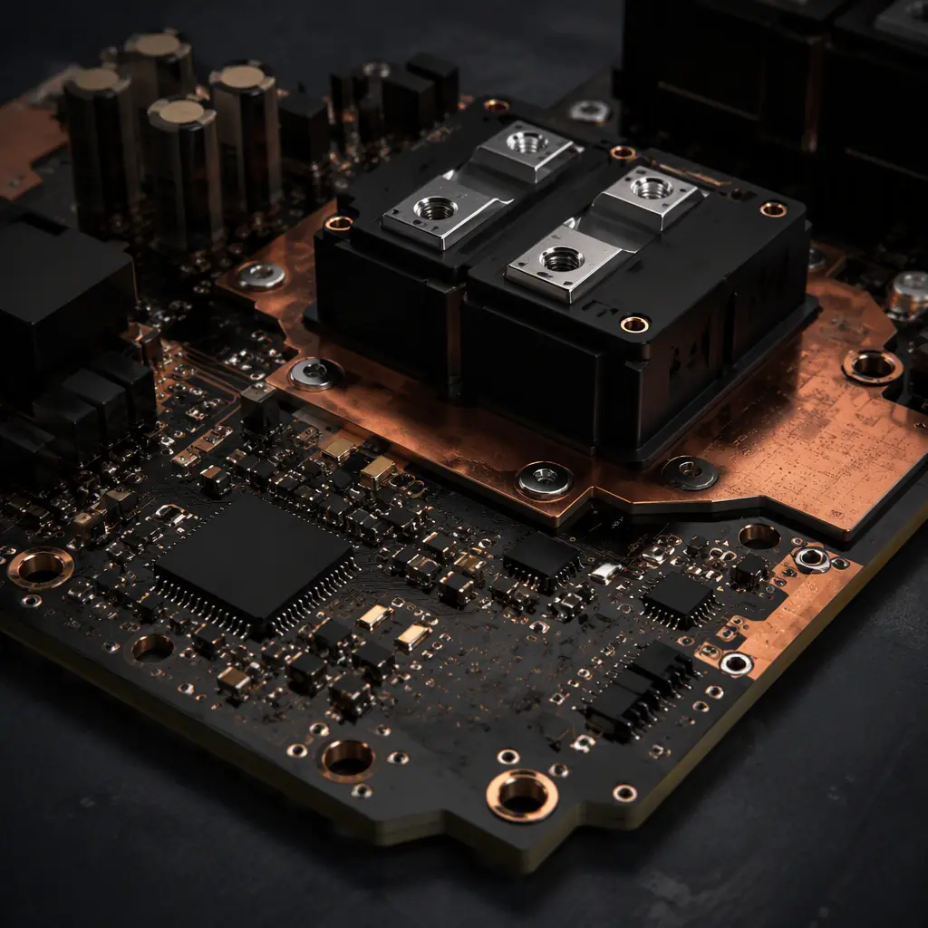
Why Wide-Bandgap Changes The Layout Rules
The headline change is speed. A silicon device might switch in 50–200 ns; a SiC or GaN device can switch in 10–40 ns. That speed is the whole point, less switching loss, higher efficiency, but it also turns the board into a transmission line with real inductance, capacitance and radiated energy.
Faster Edges Raise dV/dt And di/dt
A 100 V/ns edge across a 10 nH loop inductance generates 1 V of induced drop, which is enough to upset a gate. The same edge coupled to a neighbouring trace becomes common-mode noise that fails EMC. Every increase in edge rate must be matched by a decrease in loop inductance.
Switching Losses Move To The Board
Wide-bandgap devices are more efficient, but the current they switch still has to flow through the PCB copper. At 200 A, a trace with too little copper heats; a power stage with poor thermal management will de-rate fast. The board has to carry both the current and the heat away.
The Gate Drive Loop
The gate loop is where wide-bandgap designs most often go wrong. A fast-switching device needs its gate-driver output and its source-return path to be as close and as tight as possible. A loop that is too large behaves like an inductor that fights the driver and invites parasitic turn-on.
Keep The Driver Right Next To The Gate
Place the gate resistor and the driver output within a few millimetres of the device gate pin. The goal is a gate-loop inductance of a few nanohenries or less; every additional centimetre of trace adds inductance and slows the edge.
Return It Directly Under The Drive
Run the source-return path directly parallel to the gate trace, on the layer beneath or beside it, so the loop has the smallest area. A dedicated return alongside the gate effectively halves the inductance compared with a return that runs elsewhere on the board.
Use A 4-Layer Stackup With A Clean Reference
A solid ground plane underneath the gate-drive region gives the loop a tightly coupled return and also shields the sensitive drive from the noisy power stage. Our stackup design guide shows how to set up the layer structure.
Loop Inductance And The Switching Node
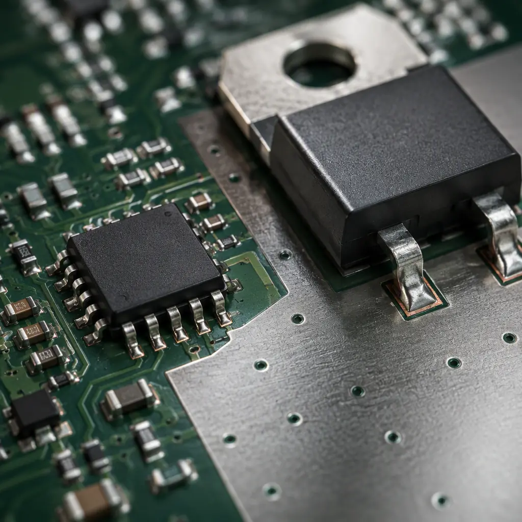
The power loop, from the DC bus capacitor, through the switch and back to the capacitor, carries the highest di/dt. Its inductance is the number-one source of voltage overshoot at turn-off and of radiated EMI.
Minimise The Power Loop Area
Place the DC-link capacitors as close to the switch and return as possible, and route the high-current path and its return as a parallel pair. Every square millimetre of loop area is inductance that becomes a voltage spike when the device turns off.
Add A Dedicated Snubber Capacitor
A small ceramic capacitor physically right at the device terminals absorbs the first spike before it circulates around the board. Place it inside the main loop, not bolted to the far side of the power stage where its lead inductance makes it useless.
Size The Copper For The Current
The current path needs enough copper to stay cool without ballooning the board. A rough guide is 300–500 mils of trace width per amp for a 2 oz outer layer, but the faster way is to use our trace width & current capacity guide to match copper to the real RMS current.
High dV/dt EMI And Common-Mode Current
The fast edges that make wide-bandgap efficient are the same edges that generate EMI. The switching node has a large voltage swing at extremely short rise time, and it capacitively couples into any conductor that runs parallel to it, heat sinks, the gate trace, the shield, even the PCB inner layers.
Keep The Switching Node Compact
Minimise the copper area of the switching node so there is less surface area to couple into the rest of the board. A small, tight switching-node pour with a ground plane under it reduces both radiated and common-mode emission.
Add A Common-Mode Filter On The Interfaces
Put a common-mode choke and proper filtering on the input and output connections so the noise does not leave the board on the cables. This is where an EMI and compliance strategy pays off, see our EMC / EMI compliance guide.
Think About The Heat Sink
A heat sink bolted over the switching node can act as an unintended capacitor. Use an insulating pad with controlled thermal conductivity and think about how much of the switching-node voltage couples into the metal. Particularly if the heat sink is bonded to the enclosure.
Thermal Management For The Power Corner
A wide-bandgap device is small and efficient, but the heat it produces is concentrated into a tiny area, and the board has to get that heat off the pads and into the heat sink. The thermal path through the PCB is the decisive factor.
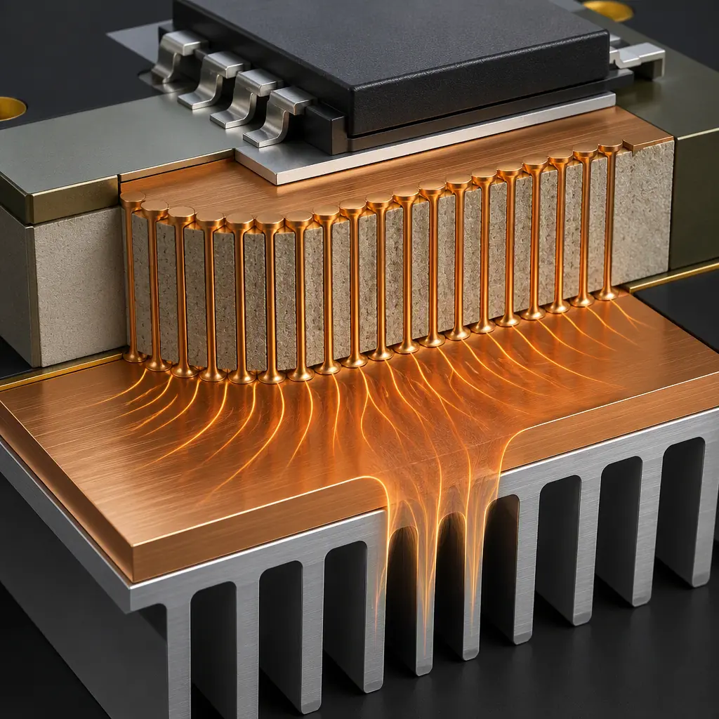
Use A Thermal Via Array Under The Device
The most effective way to move heat down through a power device's thermal pad to the copper on the far side is a dense grid of thermal vias. A good rule is a via every 1.27 mm (0.050 in) across the thermal pad, filled or tented as the process allows, with a large copper pour on the bottom layer to spread the heat. See our via technology guide and thermal management guide.
Expose Copper And Use A Low-Resistance Bond
A soldered thermal pad straight onto a copper pour has a far lower thermal resistance than a connection through a thick dielectric. For power stages, consider a heavier copper weight and a thick pad to spread the heat into the substrate. Our copper weight guide shows the options.
Match The Laminate To The Junction Temperature
High-Tg and high-Td laminates hold their mechanical and electrical integrity at the junction temperatures a SiC device can reach. A general-purpose laminate can soften where the board meets the metal pad, and it may also de-rate its insulation at speed. High-Td material with a good thermal conductivity is the safe call for a power design that does not want to trim the margin.
Creepage And Clearance At 800 V
A wide-bandgap design at 800 V bus voltage is a high-voltage design, and the board has to respect creepage and clearance on every path between the live side and the low-voltage side. Getting this wrong is a safety and EMC failure, not just a reliability nuisance.
Size Creepage To The Working Voltage
Creepage is the distance along the surface between two conductors, and it scales with voltage, the pollution degree and the material's CTI. For an 800 V bus in a harsh environment, the required surface distance is well over 8 mm typically. Use our creepage and clearance guide to set the distances for your voltage and pollution degree.
Use A Slot Or A Ruled Surface For Isolation
Where a compact board cannot afford the creepage, a milled slot or a ruled groove breaks the continuous surface and increases the effective creepage length. This is a common trick on power stages that need isolation between the high-voltage bus and the controller.
Choose A Material With A High CTI
The Comparative Tracking Index (CTI) of the laminate determines how well it resists surface tracking. A high-CTI material allows a shorter creepage distance for the same voltage, which helps in a compact design. Factor this into your laminate pick alongside the thermal-integrity requirement.
Summary. Design The Board Like It Is Part Of The Circuit
Wide-bandgap design is a board-level discipline. Keep the gate loop a few nanohenries, keep the power loop tight and the DC-link capacitors close, keep the switching node small and shielded, move the heat out with a dense thermal via array on a high-Tg laminate, and respect creepage for the voltage you are running at. Do that and the SiC or GaN device stays efficient and easy to certify.
At Huaxing PCBA we manufacture power-electronics boards with 6 oz copper, high-Tg and high-Td thermal laminates, thermal via arrays and IPC-A-610 Class 3 assembly on 8 SMT lines. Our engineers will review your gate loop, power loop and creepage budget before we quote. Send your Gerber and BOM or talk to a power-electronics engineer about your SiC or GaN design.
