
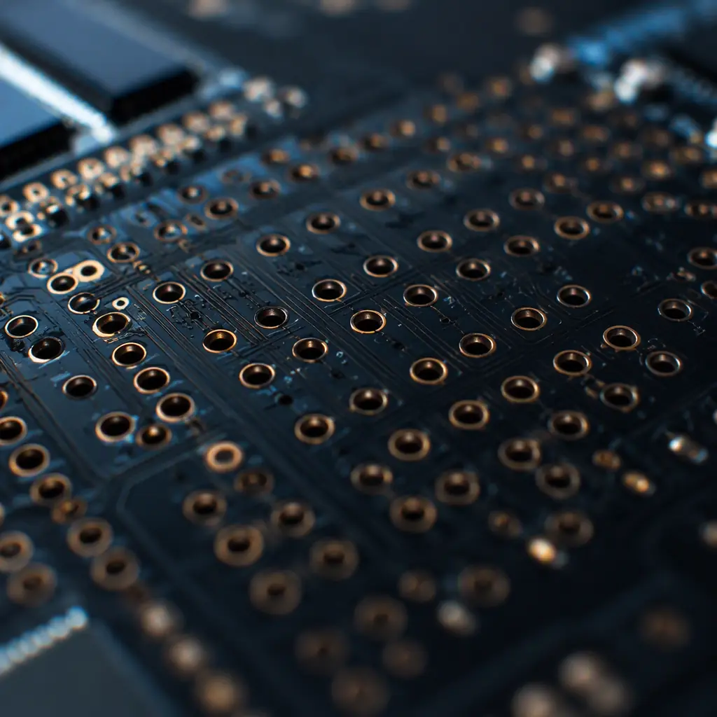
Every via on a board is a promise: the copper inside will connect one layer to another for the life of the product. But the copper that lines the barrel of a via is plated, not solid metal, and plating a tall, narrow hole is fundamentally harder than plating a short, wide one. The ratio between a via's depth and its diameter, the aspect ratio . Is the single number that determines whether that promise is easy or borderline impossible to keep.
This matters to a buyer because it is a hard physical constraint, not a matter of willingness to try. A manufacturer that says "yes, we can plate a 12:1 aspect ratio through via" without caveat is either guessing or setting you up for a yield problem. At Huaxing PCBA we drill 0.15 mm mechanical holes and 0.075 mm laser microvias on boards up to 32 layers, and aspect ratio is part of how we quote each job.
What Aspect Ratio Actually Means
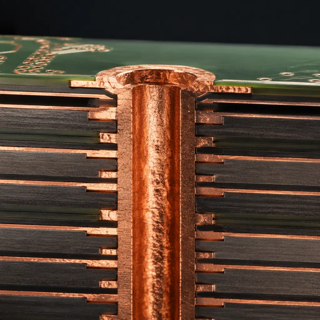
Aspect ratio is the depth of the via divided by its drilled diameter. A via that is 1.6 mm deep and 0.3 mm in diameter has an aspect ratio of roughly 5:1. A via that is 2 mm deep and 0.2 mm in diameter is 10:1. The higher the number, the harder it is to get copper down the length of the barrel and to do it evenly.
The reason is plating physics. Electrolytic copper plating deposits from the ends of the hole inward, so the centre of a deep barrel is the last place to get copper. In a very high aspect ratio via, the copper at the middle can be thin, barrel-shaped deposits, or even incomplete, producing a weak link that reads fine on a two-point continuity test and fails under thermal cycling or a current surge.
The Real-World Limits
Practical plating limits vary by process, but the bands below are a useful rule of thumb for a standard manufacturer. Treat them as a starting conversation, not an absolute. The exact number depends on barrel plating capability, the electrolyte, and the practical hole depth.
| Via type | Typical maximum aspect ratio | Notes |
|---|---|---|
| Through via (standard) | Up to ~8:1 reliably | Beyond this yield drops and testing needs care |
| Through via (advanced) | 10:1–12:1 with pulsed plating | Needs process capability; cost and risk rise |
| Blind via | Usually 0.75:1–1:1 | Blind vias are shallow by construction |
| Micro via (laser) | Typically ~0.75:1–1:1 | Very shallow; HDI any-layer is where they stack |
Microvias are a special case because they are deliberately shallow. A laser-drilled microvia is typically about as deep as it is wide. The low aspect ratio is exactly why they plate so cleanly, and it is why HDI any-layer construction, which stacks shallow microvias layer by layer, can achieve connectivity that a single deep through-via never could. Our via technology guide compares the constructions.
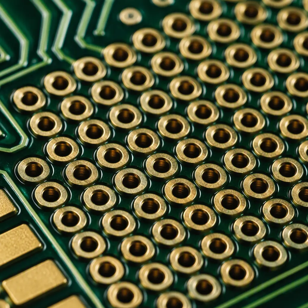
Why High Aspect Ratio Is A Reliability Risk
There are three concrete failure mechanisms to keep in mind when you are tempted to push a narrow via through a thick board:
Thin middle barrel plating
The centre of a tall via is the last to plate and is the thinnest. Under a current surge, that thin section is the hot spot and the first to fail. Current-carrying vias need the most attention, see our trace width and current capacity guide.
Incomplete plating, void in the barrel
An unplated or weakly plated pocket in the barrel is an electrical and mechanical discontinuity. It can pass a low-current continuity test and open under load or heat.
Stress and cracking under thermal cycling
The coefficient of thermal expansion mismatch between the copper barrel and the laminate subjects a via to fatigue every time the board heats and cools. A tall via has more length to accumulate that stress, so the risk rises with aspect ratio. This is why microvia reliability testing and thermal cycling matter.
What To Do When You Need To Go High
If your design genuinely needs a high aspect ratio, a thick board with a lot of layers and no room to widen the holes, there are structured ways to manage it rather than just hoping:
Talk to the manufacturer before you freeze the stackup
The aspect ratio limit is set by the plating line and the board thickness. Ask for the supported ratio for your finished board thickness up front, not after the design is locked.
Reduce the depth, not just widen the hole
Splitting a tall through via into a buried or a set of stacked microvias reduces the deepest single barrel. This is the HDI route, and it changes the whole stackup conversation. Our stackup design guide walks through the trade-off.
Backdrill long through vias that carry high-speed signals
Where the problem is a signal, not a current, backdrilling removes the unused stub and improves the signal path. See our backdrilling guide.
Verify with cross-section, not just continuity
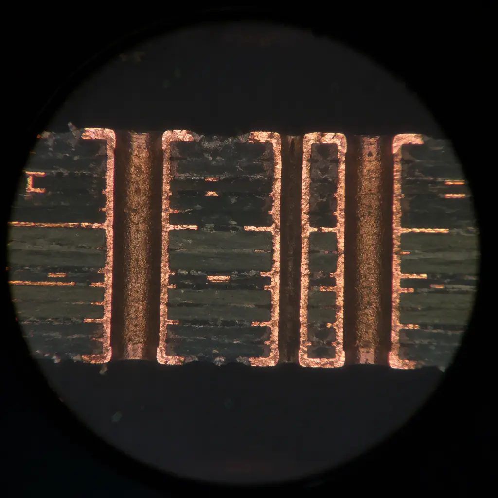
A continuity test proves the via conducts today; only a cross-section microsection shows the barrel plating thickness. For anything at the edge of the capability, drive the microsection analysis to prove the barrel is sound.
The 10-Second Buyer's Checklist
Key Takeaway: Aspect ratio is the physical constraint that decides whether your stackup is manufacturable and reliable. Keep through vias within your manufacturer's proven plating range, use blind and stacked microvias instead of one very deep hole when density demands it, and verify barrel plating with a microsection rather than trusting a continuity pass. If a quote says "we can plate 12:1" without qualification, ask for the test data.
Summary, Design Within The Plating Envelope
A via is a plated barrel, and the plating has a ceiling. The smart design move is not to push against that ceiling and hope, but to understand it early, structure the stackup so every via stays inside the proven range, and verify the result with the right measurement. That turns a yield surprise into a routine.
At Huaxing PCBA we drill 0.15 mm mechanical and 0.075 mm laser microvias on boards up to 32 layers with any-layer HDI and controlled impedance of ±5%. We review your via strategy and stackup against plating capability before you commit, so the board we quote is the one we can ship. We are ISO 9001, IATF 16949 and UL certified. Upload your files for a quote or talk to a project manager about your via and stackup strategy.
