

If you have ever returned a batch of boards because one in twenty failed at the customer site, you have more than a hunch about solder joints: the most common single root cause of PCBA field returns is a solder-related defect. It is not the components, not the design, and not the laminate. It is the metal bridge that should have connected two things and did not quite do its job.
The reason this matters so much to an overseas buyer is that solder defects are the one category you can actually verify at incoming inspection before the boards enter your product. A trace that is marginally too thin is effectively invisible to you; a solder bridge or a void under a BGA pad is not. At Huaxing PCBA we run 8 SMT lines down to 0201 and 0.3 mm pitch BGA, releasing roughly 5,000,000 placement points per month, and we will show you the AOI and X-ray images for any batch. Which is exactly what this guide teaches you to request.

The Four Defects That Actually Reach The Field
Not every cosmetic imperfection is a defect, and not every defect will fail in the field. In practice, four solder conditions account for the overwhelming majority of soldering-related returns. Understanding what each looks like and why it happens tells you where to spend your inspection budget.
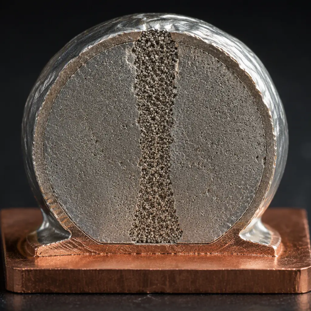
Voids, gas pockets trapped in the joint
A void is a gas pocket left inside the solidified solder. Small ones are harmless, but a large void under a BGA or QFN pad reduces the mechanical and thermal path, and concentrated voids under a power pad can drive the part into a hot spot. Voids come from trapped flux volatiles, pad coverage, paste printing and the reflow profile. Our reflow profile optimization piece covers the profile side.
Bridging, solder shorts two adjacent pads
A bridge connects two pads that should be isolated, and on fine-pitch parts it is the classic failure. It usually comes from stencil design or aperture ratio, paste volume, or an over-aggressive reflow that lets solder flow beyond the pad. This is one of the clearest AOI catches, and one of the most preventable with good stencil engineering, see our SMT stencil design guide.
Cold / disturbed solder joints, the invisible failure
A cold joint has a dull, grainy, reflowed-again look and a poor metallurgical bond. It passes visual sometimes and fails electrically months later under vibration or thermal cycling. Cold joints come from insufficient peak temperature, too short time above liquidus, or a board that moved during reflow. This is why thermal cycling testing is so revealing.
Tombstoning, the component stands up
Tombstoning happens when one side of a chip component wets faster than the other and lifts the part upright. It is usually a soldering-balance problem driven by uneven pad size, paste volume, or an asymmetric thermal footprint, and it is very common on passives. Good design-for-assembly practice prevents most of it at the layout stage.
What IPC-A-610 And J-STD-001 Actually Allow
This is the part most buyers skip, and it is the difference between an inspection that protects you and one that just looks busy. IPC-A-610 defines the visual acceptance criteria for soldered assemblies; J-STD-001 defines the process and how the solder joint must be formed. They are complementary, and a supplier quoting "IPC-A-610 Class 3" without J-STD-001 is telling you half the story. Our IPC standards comparison maps the whole family.
Two points matter most for a buyer:
Class 2 vs Class 3 changes what is acceptable
The same visual condition is often acceptable at Class 2 and a defect at Class 3 (and vice-versa for the opposite extreme). If your product is automotive, medical or aerospace, the difference is not academic. Read our Class 2 vs Class 3 comparison to know where your product sits.
BGA voiding is capped, not eliminated
For ball-grid arrays, IPC-A-610 sets practical void limits (typically a maximum void percentage per ball and a total count limit). "Zero voids" is not a realistic spec and a supplier who promises it does not understand reflow. What matters is that the void limit is written down, measured, and reported on the X-ray.
| Defect | Primary cause | Best inspection | Prevention lever |
|---|---|---|---|
| BGA void | Flux volatiles, profile | X-ray / 2D X-ray | Reball, profile, paste |
| Bridge | Stencil, paste volume | AOI | Aperture ratio, SPI |
| Cold joint | Low peak temp | AOI + reflow data | Profile validation |
| Tombstone | Thermal balance | AOI | Pad design, DFA |
How To Read The Inspection Evidence
The difference between a supplier that is confident and one that is guessing is usually the evidence they can produce. Here is the inspection stack you should expect, and what each layer tells you:
SPI (paste inspection) before reflow
If paste volume is wrong, half the solder defects are already decided before the board gets hot. A supplier running SPI (solder paste inspection) at the printer is checking volume, height and area on every paste deposit. This is a strong pre-reflow signal.
AOI (automated optical inspection) after reflow
AOI catches bridges, tombstones, misalignments and many cold joints optically, at full coverage. If the supplier reports AOI on 100% of boards, ask for the actual inspection report rather than a checkbox. Read how AOI differs from other methods in our inspection methods guide.
X-ray for hidden joints
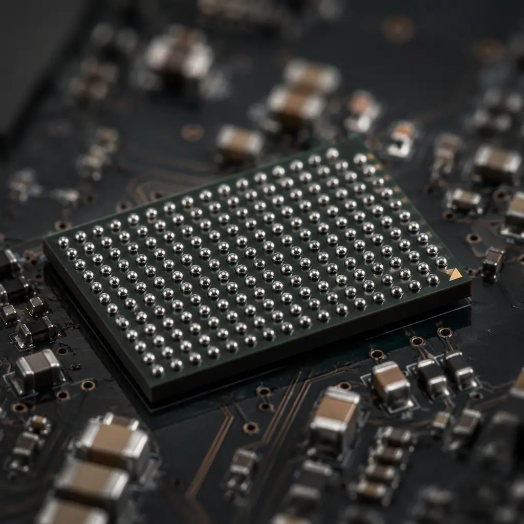
AOI cannot see under a BGA. X-ray sees voiding, bridging and missing balls under the footprint, which is why any BGA-heavy board needs it. Our BGA assembly guide covers the X-ray acceptance details.
ICT / FCT for function
Finally, in-circuit and functional test confirm the board works as a system. A cold joint that survived AOI may only be caught here. See the trade-offs in our in-circuit test vs flying probe comparison.
What To Put On Your Assembly Spec
To hold a supplier to solder quality, the requirement has to be in writing. Put the following into your RFQ and your order, so there is no ambiguity on the receiving dock:
Name the standard and the class
Write "IPC-A-610 Class 3, J-STD-001" explicitly, not "soldering per industry standard". Class is not a default and must be stated. See our certifications and compliance guide for how this fits your overall spec.
Set a measurable BGA void limit
If you care about voiding, define it: e.g. no single void above a set percentage of the pad and no total voiding above another. Do not say "no voids".
Require the inspection report
Demand AOI + X-ray summary data with the run, or proof on first article. This is covered in our first article inspection guide.
Agree on the reflow profile up front
Ask for the reflow profile to be validated and shared, especially with lead-free solder. Our lead-free vs leaded piece shows why solder alloy choice changes the profile.
The 10-Second Buyer's Checklist
Summarising the whole conversation into something you can use the next time you approve an assembly order:
Key Takeaway: Solder defects are verifiable, and they are the most common cause of returns. Ask your assembler for a stated IPC-A-610 class and J-STD-001 process, a quantified BGA void limit, and AOI + X-ray evidence on the run. If the answer to any of those is vague, treat the quote as provisional. Because the difference between a good and a failing solder joint is usually already decided before the board enters the oven.
Summary, Verify Before You Commit
The solder joint is where design, materials, paste, stencil, profile and quality systems all converge, and it is the single most inspectable point in the whole assembly. You do not need to be a metallurgist to protect yourself; you need to know which defects matter, what the standard allows, and which evidence to demand.
At Huaxing PCBA we assemble down to 0201 components and 0.3 mm pitch BGA across 8 SMT lines, with 100% AOI, SPI at the printer and X-ray for hidden joints, and we release to IPC-A-610 Class 3 by default. We are ISO 9001, IATF 16949 and UL certified, and we will walk you through the inspection data on your own boards before you pay for a single unit. Upload your files for a quote or talk to a project manager about your solder-joint acceptance criteria.
