
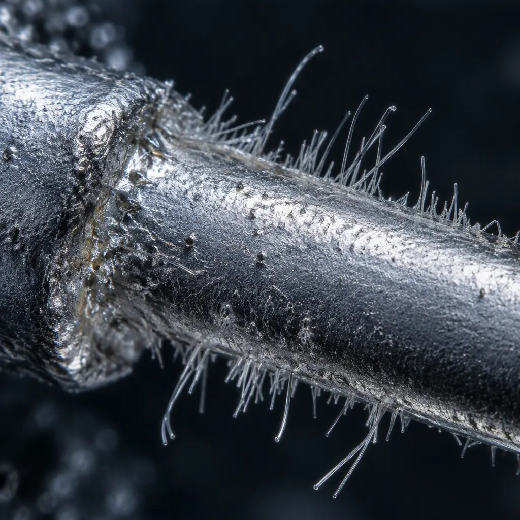
Tin whiskers are spontaneous, single-crystal tin filaments that grow out of tin and tin-alloy plated surfaces. They need no electric field to form, they grow at room temperature, and they can bridge conductors separated by several hundred micrometres. A whisker that bridges a 0.5 mm pitch component lead to its neighbour creates a short circuit that appears months or years into field service, on a board that passed every test at the factory. For any product with a long service life and a no-fault tolerance — medical, aerospace, defence, telecom infrastructure, industrial control — tin whiskers are a real reliability hazard rather than a theoretical one.
The reason this became a live issue for buyers is the transition to lead-free finishes. Pure tin and high-tin alloys are far more prone to whisker growth than the tin-lead finishes they replaced, and the 2006 RoHS restrictions put those finishes on most commercial boards. At Huaxing PCBA we build to IATF 16949 and ISO 9001 with finishes selected per programme, and for long-life programmes we ask the whisker question at RFQ stage — because by the time the finish is plated, the highest-leverage mitigation has already been decided.
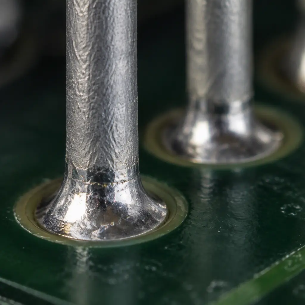
What a Tin Whisker Actually Is
A tin whisker is a filament of near-pure tin that extrudes from a plated surface. It is not a dendrite — dendrites grow electrochemically under bias in the presence of moisture and ionic contamination, and they need an electric field. Whiskers form spontaneously from the plating itself, in the absence of any applied voltage, driven by internal mechanical stress in the deposit. The distinction matters because the two failure modes have completely different mitigations: dendrites are controlled by cleanliness and by eliminating bias-driven migration, while whiskers are controlled by the metallurgy of the plating and by the mechanical stress state of the deposit.
The physical characteristics are what make them dangerous on modern boards. Whiskers are typically 1 to 5 micrometres in diameter — thinner than a human hair by an order of magnitude — and commonly 10 to 100 micrometres long, though filaments exceeding 1 millimetre have been documented in laboratory and field studies. A whisker of that length at that diameter is thin enough to be invisible under normal inspection lighting and flexible enough to survive vibration, yet it is solid metal and will carry current. On a 0.5 mm pitch device, 10 to 50 micrometres of growth is enough to bridge adjacent leads. In low-voltage, high-impedance circuits, a whisker can also be vaporised by the fault current and re-form, producing an intermittent fault that is nearly impossible to reproduce on a test bench.
Key Takeaway: A whisker is a metal filament driven by internal plating stress, not by electricity. That means it can be mitigated at the material level — by choosing a finish that does not generate that stress — which is a decision a buyer controls.
The Three Conditions That Drive Growth
Whisker growth is not random. Decades of work published through JEDEC, iNEMI and NASA's Goddard and NEPP programmes have narrowed it to three interacting drivers. A surface that satisfies none of them rarely whiskers; a surface that satisfies two or more is a candidate for a field failure.
Compressive stress inside the tin deposit is the primary driver. Tin has a body-centred tetragonal crystal structure, and when the deposit is placed under compressive stress the lowest-energy way for the lattice to relieve that stress is to extrude metal at a grain boundary. Sources of compressive stress include the intermetallic compound layer that forms between tin and a copper substrate, plating chemistry and current-density non-uniformity, thermal expansion mismatch, mechanical damage from lead forming or insertion, and corrosion of the substrate beneath the plating.
Grain structure and deposit morphology determine susceptibility. Fine-grained, bright, electroplated tin with columnar grains and high internal stress whiskers far more readily than a coarse, matte, equiaxed deposit. This is why matte tin is the recommended lead-free finish for long-life applications: the deposit is intrinsically lower-stress rather than merely thinner. Small-grained bright tin, which is aesthetically preferred and widely used on commercial components, is the worst case.
Temperature cycling and humidity accelerate growth. Thermal excursions introduce additional stress through CTE mismatch and accelerate diffusion in the intermetallic layer. Humidity drives oxidation and corrosion, which adds stress at the interface. The practical implication is that a board in a benign, temperature-stable, air-conditioned enclosure grows whiskers far more slowly than the same board in an industrial enclosure that cycles daily.
Mitigation by Finish Selection
This is the highest-leverage decision available to a buyer, because a different finish can reduce whisker propensity by orders of magnitude rather than by a few percent. It is also entirely within the buyer's control — the surface finish is a line item in the fabrication specification. The following table reflects the general behaviour reported across the JEDEC and NASA body of work.
| Finish | Composition | Whisker Risk | Best Fit |
|---|---|---|---|
| HASL, tin-lead | Sn63/Pb37 or equivalent | Very low | Solderability-critical boards where RoHS exemption applies |
| Lead-free HASL | SnCu or SnAgCu | Low to moderate | Cost-sensitive commercial boards with short service life |
| ENIG | Ni 3–6 µm, Au 0.05–0.15 µm | Very low — no exposed tin | Fine pitch, high-reliability, long life |
| ENEPIG | Ni / Pd / Au | Very low — no exposed tin | Wire-bondable + solderable, high mix |
| Immersion tin | Sn 0.8–1.2 µm over copper | Moderate to high | Fine pitch press-fit and compliant pin work |
| Immersion silver | Ag 0.1–0.3 µm | Low — but Ag migration is a separate risk | Fine pitch, high-speed signals |
| OSP | Organic film | None — no metal | Short-life, single-pass reflow, high volume |
The pattern is clear: finishes that contain no exposed pure tin are effectively immune, and finishes that are pure tin or high-tin are the ones that require process control. For a board with a fifteen-year service life, the finish specification is a far more effective mitigation than any downstream process step. Where a programme requires pure tin plating for solderability or compliance reasons, the exposure has to be managed deliberately.
Procurement Note: Specify the finish explicitly by thickness and composition, not by trade name. "ENIG" without a gold thickness range is insufficient — too much gold produces brittle solder joints, too little leaves porosity that exposes nickel and lets a tin-rich intermetallic form at the surface.
It is also worth noting that the finish on the printed circuit board is only half the picture. Component terminations arrive with their own plating, largely chosen by the component manufacturer and frequently pure matte or bright tin. A buyer who specifies ENIG for the bare board can still receive components with tin-plated leads. Our surface finish selection guide covers board-level finish choice in more depth, and our comparison of ENIG versus HASL works through the solderability consequences.
Mitigation by Process and Design
Where a tin-bearing finish is unavoidable, process and design controls reduce the risk. None of them is as clean as eliminating the tin, but taken together they move a programme from uncontrolled to managed exposure.
Specify Matte, Not Bright, Tin
Matte tin deposits are coarse-grained and lower in internal stress than bright tin, which is fine-grained and contains organic co-deposited brightening agents that increase stress. Matte tin is the default recommendation for lead-free terminations in long-life applications. When a supplier offers "tin plated" leads without qualification, ask which morphology is being supplied — the answer changes the risk profile substantially, and it costs the supplier nothing to specify the lower-risk option.
Apply Post-Plating Anneal or Reflow Fusing
Annealing a tin deposit at approximately 150 °C for one hour, or subjecting it to a reflow excursion, recrystallises the plating and relieves the internal stress that drives whisker growth. Reflow fusing during assembly achieves the same effect on the board finish as a by-product of soldering — which is one reason a lead-free HASL surface that has been through reflow is less of a whisker source than an as-plated immersion tin surface. Annealing is not a permanent cure, because new stress accumulates from intermetallic growth at the copper interface over time, but it buys a substantial delay in the growth window.
Use Conformal Coating as a Mechanical Barrier
A conformal coating does not prevent whisker nucleation, but it does contain the filament. A whisker growing beneath a cured coating will typically deflect along the coating interface rather than penetrate it, and cannot bridge an air gap between conductors. Coating is therefore an effective secondary mitigation and is commonly required by aerospace and defence programmes in combination with a whisker-mitigated finish. The caveat is that the coating must be applied after all soldering and forming operations, and it must be continuous over the features at risk. Our conformal coating guide and our article on masking techniques cover the process requirements.
Design Keep-Outs for Whisker-Susceptible Geometry
Whisker-induced failures happen where fine-pitch conductors sit at different potentials and where a bridge would be consequential. Layout mitigations include increasing spacing beyond the whisker growth envelope on high-voltage and high-impedance nets, avoiding long parallel runs of tin-plated leads at minimum pitch, and routing sensitive nodes away from tin-plated hardware such as card guides and chassis fasteners. Where a bridge is unavoidable, a series resistor or a current-limited node converts a hard short into a recoverable fault. These are design-stage decisions that cost nothing once taken and are expensive to retrofit.
Control Storage and Handling Stress
Mechanical damage introduces stress. Lead forming, insertion force, board depanelisation stresses and rough handling all compress the plating locally and can seed whisker growth at those points. Bent-lead soldering should be specified with controlled force, and press-fit insertion — which by design compresses the plated barrel — leaves a highly stressed tin deposit. This is one reason press-fit applications prefer a finish other than pure tin where the reliability requirement is high. Our coverage of press-fit technology addresses that interface directly.
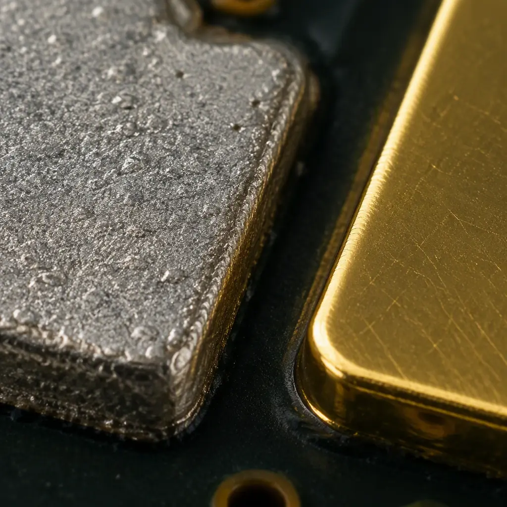
When Hot Solder Dip Is the Right Answer
For the most demanding long-life programmes, the accepted mitigation is to remove the tin entirely by hot solder dipping the component terminations in a tin-lead or tin-silver bath. Components are dipped so that their original pure-tin plating is dissolved and replaced by an alloy with negligible whisker propensity. The approach is well established in aerospace and defence supply chains, and it is the mitigation that offers the most direct control because it removes the susceptible material rather than managing its stress state.
The costs are real, and they are the reason the technique is not applied universally. Hot solder dipping requires the component to survive a molten-metal immersion, which excludes many plastic-bodied and moisture-sensitive parts. It introduces thermal shock, so moisture-sensitive devices need baking first. It cannot be applied to fine-pitch SMT parts at all — the process is practical on through-hole, axial, radial and connector terminations but not on a 0.5 mm pitch QFN. And it consumes a lead-containing alloy, which for a RoHS-compliant product requires an exemption. Where a programme cannot accept lead, a tin-silver dip is the alternative, at higher process temperature and higher cost.
The practical decision rule we apply is this: if the product has a service life beyond roughly ten years, a no-fault consequence to a bridged circuit, and terminations that can physically tolerate the dip, hot solder dip belongs in the specification. If any of those three conditions fails, a whisker-mitigated finish combined with conformal coating is the appropriate level of control.
Standards and Spec Language for Your PO
The reason whisker risk often goes unmanaged is not that the mitigations are unknown — it is that the requirement is not written into the purchase order. A supplier builds to what is specified. The following standards define both the test methods and the acceptance framework, and they give you ready-made language.
| Standard | Scope | When to Reference |
|---|---|---|
| JESD22-A121 | Whisker growth test method — environmental sequences, inspection interval, acceptance | Any programme requiring documented whisker testing |
| JESD201 | Environmental acceptance requirements for whisker susceptibility of tin finishes | Qualifying a finish or a supplier for long-life use |
| JESD22-B105 | Whisker test by board-level thermal cycling | Board-level rather than component-level verification |
| GEIA-STD-0005-2 | Standard for mitigating tin whisker effects in aerospace and high-performance electronics | Aerospace and defence programmes |
| NASA-STD-8739.8 / NEPP guidance | NASA's whisker mitigation recommendations and prohibition of pure tin where applicable | Space and mission-critical work |
| IPC J-STD-001 | Soldering requirements including coating and cleanliness that support whisker mitigation | General assembly specification |
A workable PO clause is short. It states the finish by composition and thickness, prohibits pure bright tin on terminations where a suitable alternative exists, requires matte morphology where tin is unavoidable, requires a post-plating anneal or specifies that reflow fusing is acceptable, requires conformal coating over whisker-susceptible features where the product class demands it, and references JESD22-A121 for any test evidence requested. Adding that paragraph to a specification costs nothing and gives the supplier a clear, verifiable requirement — which is the only way the mitigation actually reaches the product. Our article on certifications and compliance covers how these requirements sit alongside RoHS and REACH obligations, and our solderability testing guide covers the verification side.
Key Takeaway: Whisker mitigation is a specification problem before it is a manufacturing problem. Choose a tin-free finish where the service life justifies it, require matte morphology and annealing where tin is unavoidable, add conformal coating as a barrier, and write the requirement into the PO with a named standard. Unwritten requirements are not met.
Summary and Next Steps
Tin whiskers are a genuine long-term reliability hazard in lead-free assemblies, and they are unusual among reliability risks in that the most effective mitigation is a purchasing decision rather than a process capability. Selecting a finish that contains no exposed tin eliminates the failure mode. Where tin is required, matte morphology, a post-plating anneal, conformal coating as a barrier and layout spacing rules together reduce the risk to a managed level. Hot solder dip remains the strongest mitigation for the most demanding programmes, at a process cost that makes it a deliberate choice rather than a default.
At Huaxing PCBA we fabricate and assemble boards with the full range of finishes — lead-free and tin-lead HASL, ENIG, ENEPIG, immersion silver, immersion tin and OSP — and we discuss whisker mitigation with customers at RFQ stage for medical, aerospace, defence and long-life industrial programmes. We can apply conformal coating over whisker-susceptible features, provide finish thickness data for your records, and build to specifications that reference JESD22-A121 or GEIA-STD-0005-2. Send your Gerber, BOM and reliability requirement, and our engineering team will respond within 24 hours with a finish recommendation, a free DFM review and a quote. You can also read our comparison of lead-free and leaded assembly or contact our engineering team to discuss a specific programme.
