

Huaxing PCBA PCB manufacturing insights and articles

Insights & Resources

Technical articles on PCB design, manufacturing, and industry best practices. Written by our engineering team.
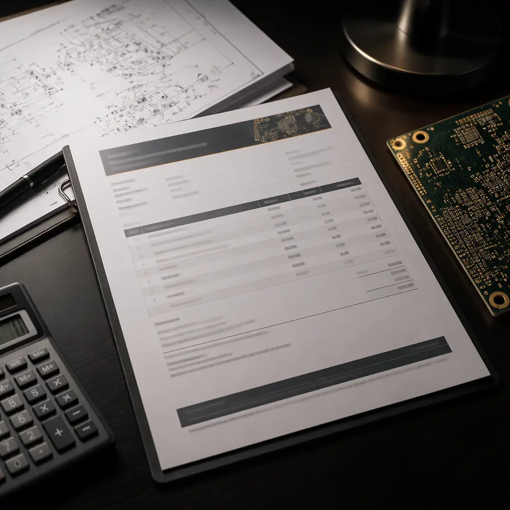
How to Read a PCB Quotation — Line-by-Line Cost Breakdown

How to Read a PCB Quotation — Line-by-Line Cost Breakdown

Learn to decode every line in a PCB quotation: where hidden costs hide, which line items are negotiable
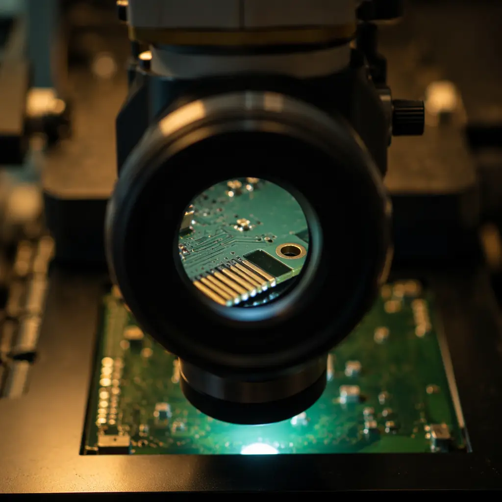
How to Resolve PCB Quality Disputes — IPC Standards, Lab Testing & Negotiation Framework

How to Resolve PCB Quality Disputes — IPC Standards, Lab Testing & Negotiation Framework

Practical framework for resolving PCB quality disputes: how to use IPC-A-600 and IPC-6012 as contract tools
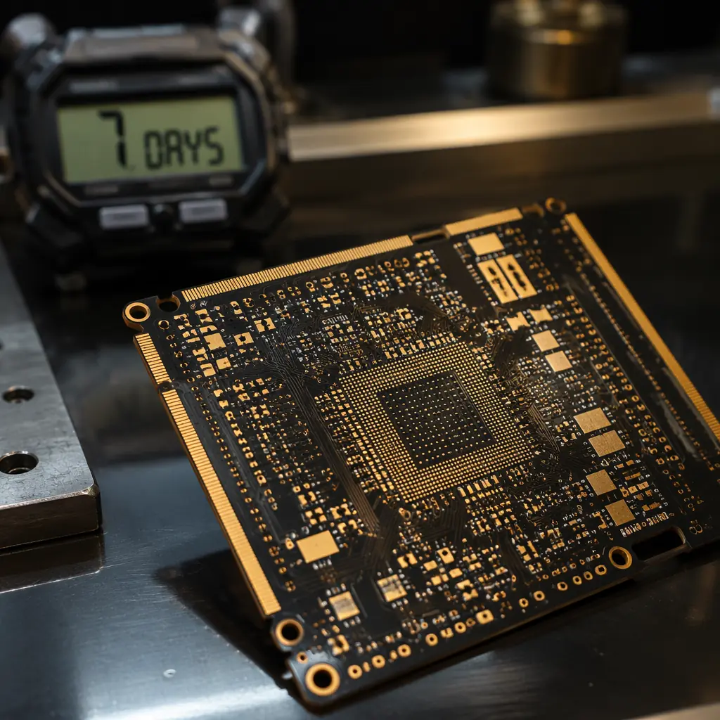
PCB Lead Time Reduction — A Procurement Manager's Guide to Faster Delivery Without Sacrificing Quality

PCB Lead Time Reduction — A Procurement Manager's Guide to Faster Delivery Without Sacrificing Quality

Reduce PCB lead times from 4 weeks to 7 days. Covers design decisions that cut days: material selection impact, quick-turn vs standard economics
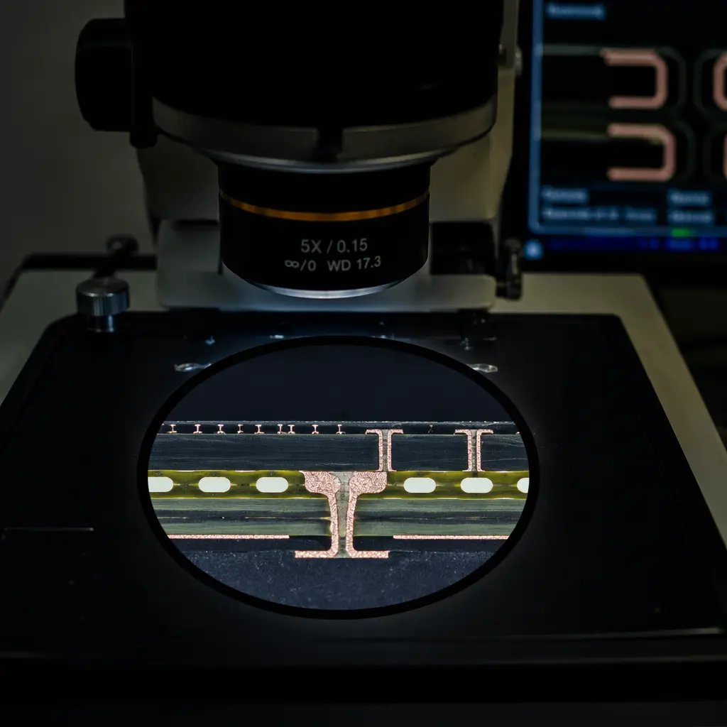
PCB First Article Inspection Guide — What Buyers Must Verify Before Mass Production

PCB First Article Inspection Guide — What Buyers Must Verify Before Mass Production

A procurement manager's guide to PCB First Article Inspection (FAI) and how to structure FAI reports that catch issues before 10,000 units ship

PCB Design for EV Charging Infrastructure — Power Electronics for AC and DC Fast Charging Stations

PCB Design for EV Charging Infrastructure — Power Electronics for AC and DC Fast Charging Stations

PCB requirements for AC Level 2 and DC fast charging stations: high-current power distribution, thermal management for 350kW+ chargers, galvanic isolation
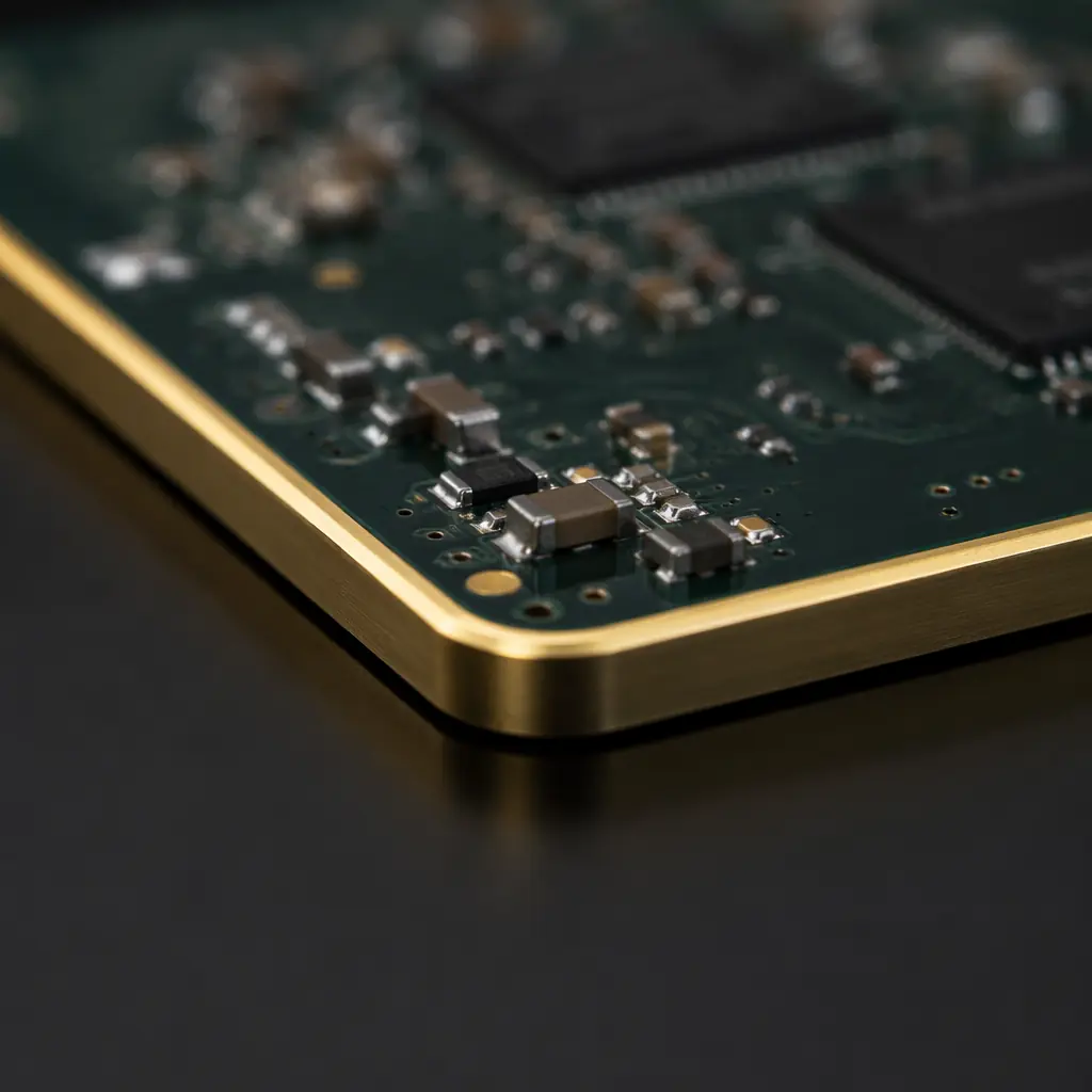
PCB Edge Plating & Castellations Guide — Sidewall Metallization for IoT Modules

PCB Edge Plating & Castellations Guide — Sidewall Metallization for IoT Modules

PCB edge plating and castellated hole design guide covering sidewall metallization vs half-holes, minimum web specs and copper-to-edge clearance
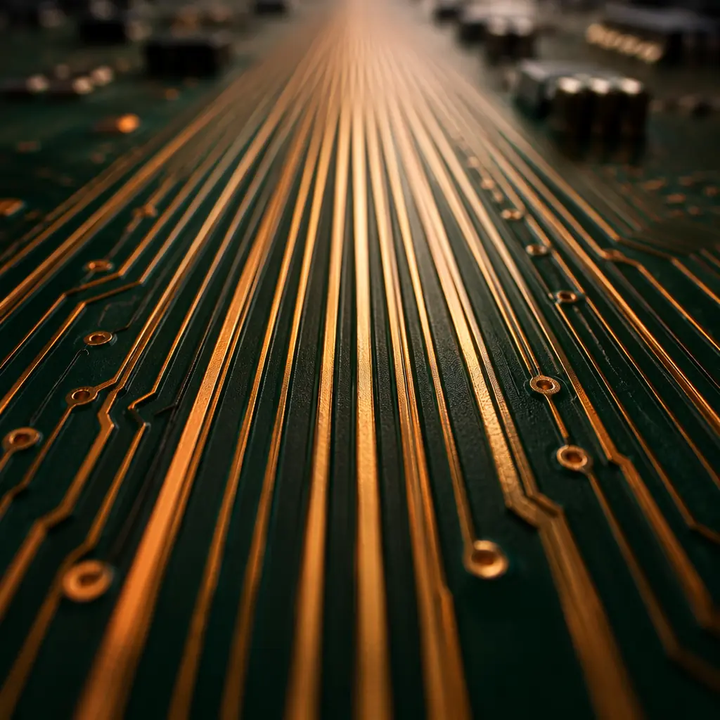
PCB Crosstalk Analysis & Mitigation — Near-End vs Far-End, Guard Traces & Stackup Strategies

PCB Crosstalk Analysis & Mitigation — Near-End vs Far-End, Guard Traces & Stackup Strategies

Complete PCB crosstalk analysis guide covering near-end (NEXT) vs far-end (FEXT) coupling mechanisms, guard trace effectiveness, differential pair spacing
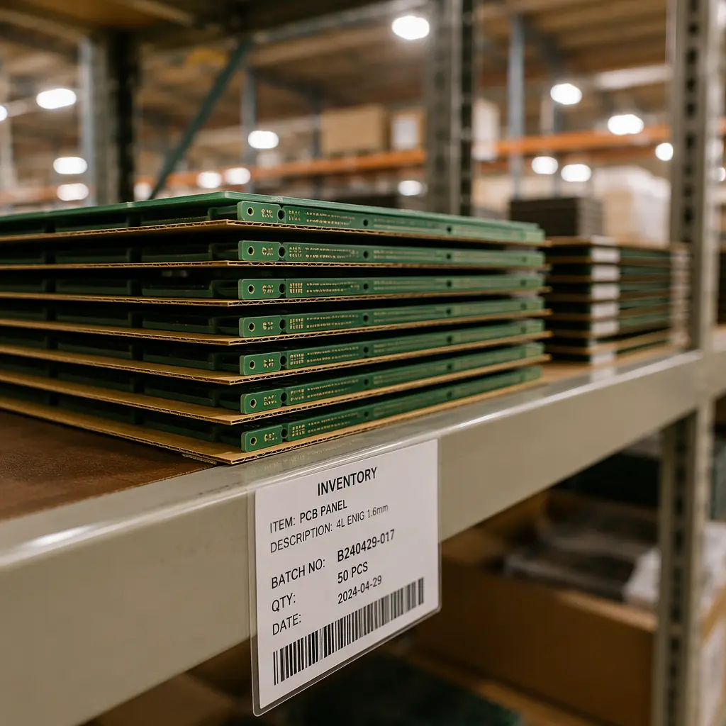
PCB Blanket Orders vs Spot Buys — Which Procurement Strategy Saves More

PCB Blanket Orders vs Spot Buys — Which Procurement Strategy Saves More

Compare blanket order vs spot buy for PCB procurement, and a decision framework for which strategy fits your production profile
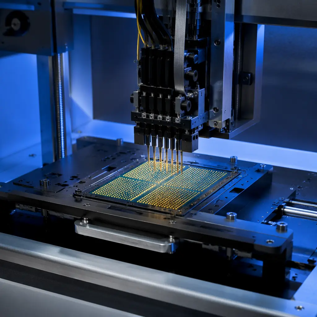
PCB for Semiconductor ATE & Test Equipment — Load Boards, Probe Cards & Burn-In Board Manufacturing Requirements

PCB for Semiconductor ATE & Test Equipment — Load Boards, Probe Cards & Burn-In Board Manufacturing Requirements

Technical sourcing guide for ATE load boards: probe cards, and burn-in boards, 40+ layer stackups, ±5% impedance tolerance, polyimide/BT/ceramic materials
Page 38 of 49