
The global EV charger market is installing hardware at a rate of 20,000+ public charging points per week. Every one of those chargers contains at least one power electronics PCB, and in DC fast chargers, typically 8-12 power modules, each with its own high-current PCB. The total addressable PCB market for EV charging infrastructure passed $1.2 billion in 2025 and is growing at 25% CAGR. But the PCB requirements are unlike anything in conventional power electronics.
This article covers the PCB-level design rules for EV charger power modules: AC Level 2 (3.3-22kW), DC fast charging (50-350kW), and the emerging megawatt charging system (MCS) for heavy-duty vehicles. It is written for power electronics engineers designing charger hardware and procurement teams sourcing PCB manufacturing for charger OEMs.
The PCB Challenge: High Power Density in a Sealed Outdoor Enclosure
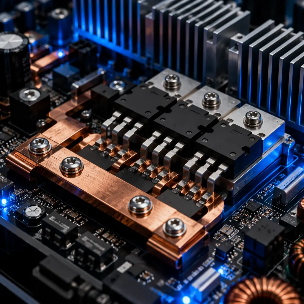
An EV charger power module is a study in conflicting requirements. It must deliver 30-60kW per module (stacked for higher total output) in a form factor that fits inside a sealed, fan-cooled outdoor enclosure. The PCB is simultaneously a structural element (supporting heavy magnetics and heatsinks), a thermal path (conducting heat away from SiC MOSFETs switching at 50-100 kHz), and a high-voltage isolation barrier (separating 800V DC bus from control electronics).
The thermal math: A 30kW power module operating at 96% efficiency dissipates 1,200W of heat. On a 250×150mm PCB, that is 3.2 W/cm² . Roughly the heat flux of a stovetop burner at medium setting. Natural convection in a sealed enclosure cannot remove this. The PCB itself must serve as a thermal spreader, moving heat from semiconductor junctions to heatsink interfaces through copper pours, thermal vias, and, in the highest-power designs, embedded copper coins.
Unlike indoor industrial electronics, EV chargers face outdoor environmental stress: -30°C to +50°C ambient, IP54 or IP65 enclosure sealing, direct solar radiation adding 10-15°C to internal temperature, and condensation when ambient temperature rises faster than the enclosure interior. These conditions accelerate every PCB degradation mechanism, CAF growth, solder joint fatigue, and partial discharge in high-voltage clearances.
AC Level 2 Charger PCBs (3.3-22kW)
AC chargers are the simpler case, they deliver AC mains power to the vehicle's onboard charger. The PCB primarily handles: contactor control, residual current detection (RCD), PWM communication per IEC 61851-1, and safety interlocks. Power levels are modest (32A at 240V single-phase or 32A at 400V three-phase).
But "simpler" does not mean trivial. The PCB must:
Maintain Creepage Distances for 400VAC
IEC 61851-23 requires 6mm creepage for reinforced insulation at 400VAC (pollution degree 2, material group IIIa). This is significantly larger than standard PCB design rules allow between adjacent pins on a relay or contactor footprint. Layout must explicitly verify creepage paths, not just clearance, around every high-voltage node.
Survive 6kV Surge (IEC 61000-4-5)
AC chargers connect directly to the grid and face lightning-induced surges. The PCB must withstand 6kV common-mode and 3kV differential-mode surges without arc-over. This requires surge-rated clearance distances and, critically, spark gaps or gas discharge tubes at the AC input, not something a standard industrial PCB design includes by default.
Functional Safety Isolation
The control PCB straddles two domains: the high-voltage AC side (contactor coil drivers, voltage sense dividers) and the SELV (Safety Extra-Low Voltage) side (microcontroller, communication interfaces). The isolation barrier between them must withstand 3,750 VAC for 1 minute per IEC 61851-23. This is typically implemented with a physical isolation slot in the PCB, a routed air gap, not just creepage distance on a continuous substrate.
DC Fast Charger PCBs (50-350kW)
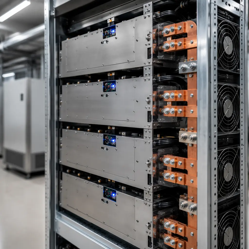
DC fast chargers bypass the vehicle's onboard charger and deliver DC power directly to the battery. This requires power conversion from grid AC to high-voltage DC: typically 200-1000V at 100-500A. The PCB inside each power module handles this conversion and faces challenges that push PCB manufacturing to its limits.
Heavy copper is not optional. At 500A output current, even a 10mm-wide, 6oz copper trace has a resistance of 0.5 mΩ/cm, dissipating 125W per meter of trace. Standard 1oz copper (35 μm) is simply not in the conversation, the trace would need to be 60mm wide to carry 500A at a 10°C temperature rise, which is wider than many power module PCBs. 4oz to 6oz copper on outer layers is the baseline for DC charger power stages.
Huaxing PCBA's heavy copper capability supports up to 6oz copper on outer layers and 4oz on inner layers, with heavy copper PCB processes optimized for uniform plating thickness, a critical quality metric when trace cross-section directly determines current-carrying capacity.
SiC and GaN: The Semiconductor Shift Reshaping PCB Design
DC fast charger power modules are transitioning from silicon IGBTs to silicon carbide (SiC) MOSFETs and, increasingly, gallium nitride (GaN) HEMTs for the auxiliary power supplies. SiC switches at 50-100 kHz (vs. 8-20 kHz for IGBTs), which reduces magnetics size but introduces new PCB challenges:
| Parameter | Si IGBT (Legacy) | SiC MOSFET (Current) | PCB Impact |
|---|---|---|---|
| Switching frequency | 8-20 kHz | 50-100 kHz | Gate drive loop inductance must be <5 nH . Requires tight Kelvin-source PCB layout |
| dv/dt | 5-10 kV/μs | 50-100 kV/μs | Common-mode noise couples through parasitic PCB capacitance; guard traces with grounded shield planes are essential |
| Junction temperature | 150°C max | 175°C max | PCB substrate must survive higher local temperatures under the device; polyimide or high-Tg FR-4 with thermal vias |
| Power density | 3-5 kW/L | 8-12 kW/L | Higher density demands embedded copper coin or IMS (insulated metal substrate) for die-level heat extraction |
For mixed-signal designs with high-voltage power stages and sensitive control electronics on the same PCB, see our mixed-signal PCB design guide.
Thermal Management: The Make-or-Break Design Constraint
Thermal management of EV charger PCBs is not about picking a heatsink. It is about designing the PCB itself as a thermal system:
Thermal Vias Under Every Power Semiconductor
A 0.3mm diameter thermal via with 25 μm copper plating has a thermal resistance of approximately 120°C/W from top to bottom of a 1.6mm board. A 10×10 array of such vias under a TO-247 package footprint provides a combined thermal resistance of ~1.2°C/W . Essential when the device junction-to-case thermal resistance is 0.5-1.0°C/W and the total thermal budget from junction to ambient is perhaps 30°C. Our PCB thermal management guide covers via sizing and placement in detail.
Embedded Copper Coins for 350kW+ Modules
At power levels above 30kW per module, thermal vias alone cannot extract heat fast enough from SiC MOSFETs switching at the upper end of their frequency range. Embedded copper coins, solid copper inserts pressed into the PCB directly under the semiconductor die, provide a thermal conductivity of 385 W/m·K, compared to 0.3-0.4 W/m·K for FR-4. This is a 1,000× improvement and the difference between a 175°C Tj max SiC MOSFET running at 120°C or failing thermal shutdown at full load.
IMS (Insulated Metal Substrate) for Single-Layer Power Boards
For the simplest power stages, a single-layer high-current PCB bonded to an aluminum baseplate, IMS construction eliminates the FR-4 thermal bottleneck entirely. The dielectric layer between copper and aluminum is 75-150 μm thick with a thermal conductivity of 1-3 W/m·K, providing an order-of-magnitude better heat spreading than FR-4. IMS is well-suited to AC charger power boards and DC charger auxiliary supplies. Our metal core PCB guide covers IMS design rules.
Partial Discharge: The Hidden Killer in High-Voltage DC PCBs
At DC bus voltages above 500V, partial discharge (PD) becomes a real failure mechanism in PCB insulation. PD occurs when small voids in the dielectric, air gaps in the resin, delamination at the glass-resin interface, or voids in the solder mask, experience electric field strengths above the breakdown threshold of air (3 kV/mm). Each PD event erodes the surrounding insulation, and over thousands of events, creates a conductive carbon track that eventually results in a hard short circuit.
Design rule: For 800V DC bus designs, minimum clearance between high-voltage and low-voltage domains should be 4mm on outer layers and 2mm on inner layers, well above the IPC-2221 generic values. These numbers come from IEC 60664-1 for reinforced insulation at 800V with pollution degree 2. If your PCB supplier cannot maintain these clearances with <0.1mm registration accuracy, they cannot produce reliable 800V PCBs.
Mitigation strategies: vacuum lamination to minimize resin voids (standard in our laminate selection process), conformal coating to fill surface voids (see conformal coating guide), and, for 1500V MCS designs, potting of the entire high-voltage section. Partial discharge inception voltage (PDIV) testing per IEC 60270 verifies the design margin.
IEC 61851 Compliance: What the PCB Must Deliver
IEC 61851 is the international standard for EV conductive charging systems. Its PCB-level requirements include:
| Requirement | IEC 61851 Reference | PCB Implementation |
|---|---|---|
| Dielectric withstand | 61851-23 §9.2 | 3,750 VAC / 1 min between HV and SELV; routed isolation slot ≥2mm width |
| Touch current limit | 61851-23 §8.5 | <3.5mA AC / <10mA DC; Y-cap placement on PCB must minimize leakage |
| Over-temperature protection | 61851-23 §10.3 | NTC thermistor placed directly adjacent to hottest SiC MOSFET on PCB |
| Residual current detection | 61851-1 §11.3 | 6mA DC + 30mA AC RCD; sense winding PCB layout critical for noise immunity |
| CP / PP signal integrity | 61851-1 Annex A | ±12V PWM at 1kHz; analog front-end PCB routing with guard traces against 800V switching noise |
Production and Testing: What EV Charger OEMs Should Demand
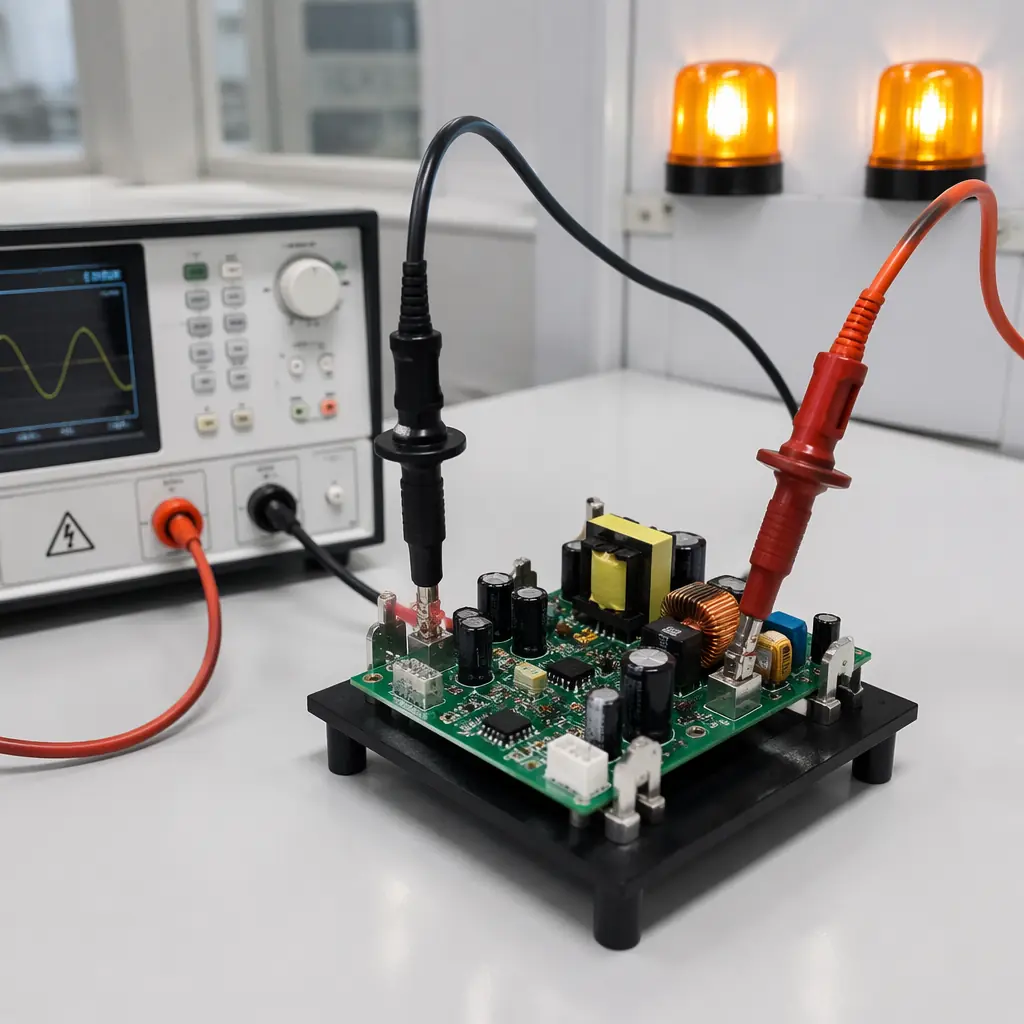
Standard PCB acceptance testing, electrical test (continuity/isolation), AOI, and visual inspection, is insufficient for EV charger PCBs. Additional production tests required:
HiPot Testing on Every Board
100% hipot testing at 3,750 VAC for 1 second (production time constraint) between HV and SELV domains. Not sampling: every board. A single hipot failure in the field means a charger that trips its RCD at installation or, worse, one that doesn't and creates a shock hazard. Our quality inspection process includes hipot as mandatory for high-voltage designs.
Partial Discharge Screening
For 800V+ designs, PD screening at 1.5× Vmax (1,200V for 800V bus) per IEC 60270. PD magnitude <10 pC is the acceptance threshold. Boards exceeding this threshold are not necessarily failed, they may pass hipot, but they carry a latent defect that will manifest as a field failure in months 18-36.
Thermal Imaging of Power Stage
At full load, a thermal camera scan of the populated PCB identifies hot spots that simulation missed, a misplaced thermal via, a component too close to a heat source, a copper pour with an unexpected current constriction. Temperature deviation from simulation by >10°C triggers a design review. See our thermal management guide for more.
The PCB Manufacturer's Capability Checklist
When sourcing PCBs for EV charger production, verify that your manufacturer can demonstrate, not claim, the following capabilities:
| Capability | Minimum Spec | Why It Matters |
|---|---|---|
| Heavy copper | 4-6oz outer, 3-4oz inner | 500A+ current paths at acceptable temperature rise |
| Copper coin embedding | Thermal conductivity >300 W/m·K | SiC MOSFET die-level heat extraction for 350kW modules |
| HiPot testing | 3,750 VAC, 100% of boards | Zero field failures from insulation defects |
| PD screening | IEC 60270, <10 pC at 1.5× Vmax | Eliminates latent insulation failures at 800V+ |
| Impedance control | ±5% on gate drive traces | Prevents SiC/GaN gate oscillation and shoot-through |
| High-Tg laminates | Tg 170°C+, Td >325°C | Survives reflow + 175°C Tj operation + safety margin |
Huaxing PCBA's 15,000㎡ Shenzhen facility supports 2-32 layer PCBs with heavy copper up to 6oz, embedded copper coin technology, and 100% electrical test plus hipot on every high-voltage board. Our IATF 16949 quality system provides the traceability and process control that EV charger OEMs require. For designs incorporating battery management, see our EV BMS PCB design guide.
