
Blog
Technical articles on PCB design, manufacturing, and industry best practices. Written by our engineering team.
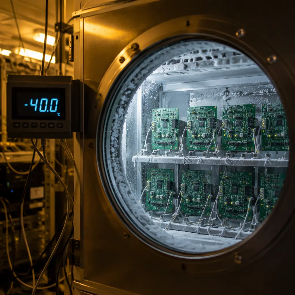
Complete guide to PCB burn-in testing and environmental stress screening: HASS vs HALT, burn-in duration by industry, MTBF prediction
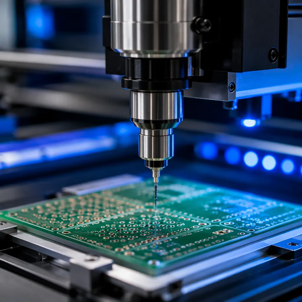
Via stubs create signal reflections that destroy high-speed signal integrity above 5 Gbps. Learn how back drilling removes stubs

Low-volume PCB assembly for 50-500 units without MOQ penalties. Covers NRE cost reduction: panel sharing, negotiation tactics
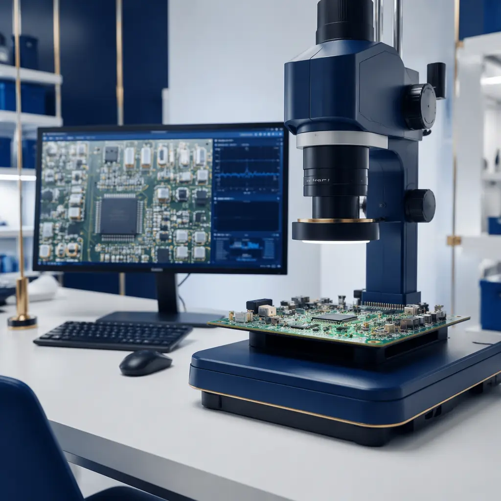
IPC-A-610: J-STD-001, and IPC-6012 serve different purposes in PCB procurement. Learn which standard to reference on your PO, how they overlap

How to manage component obsolescence in PCB assembly: EOL forecasting, last-time buy calculations, BOM health scoring, and redesign strategies for industrial
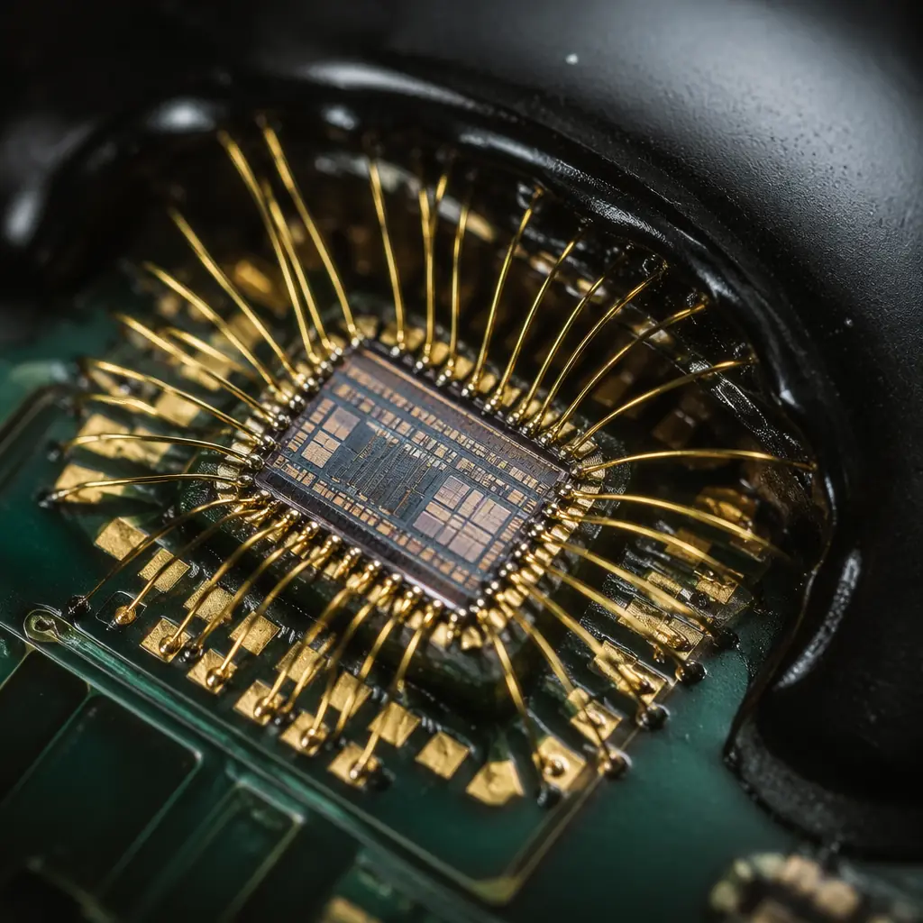
Complete comparison of COB (Chip-on-Board): COG (Chip-on-Glass), and SMT assembly technologies. Learn when to use each, wire bonding, encapsulation
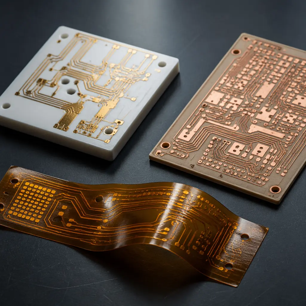
Compare ceramic (Al₂O₃, AlN): PTFE (Teflon), and polyimide PCB substrates, Dk/Df, thermal conductivity, Tg, cost, and application fit for RF, aerospace
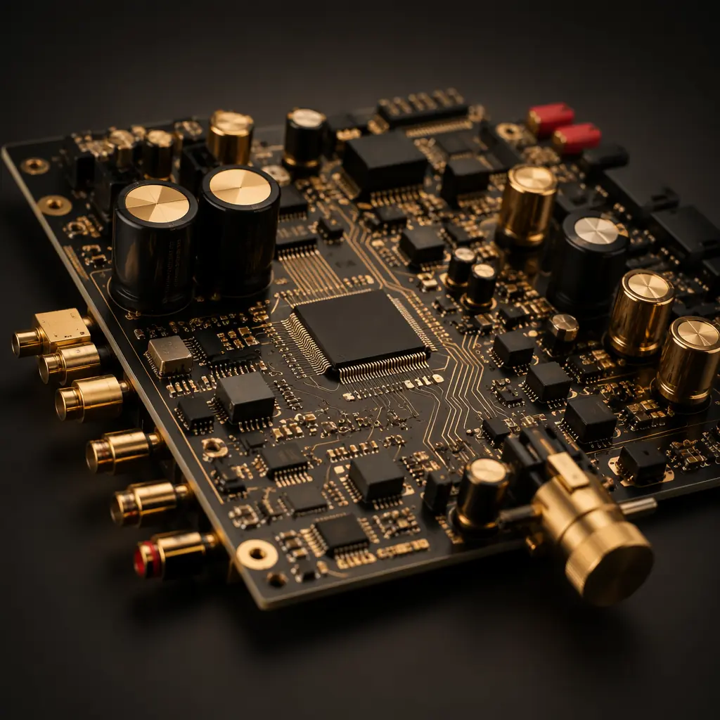
How PCB design and manufacturing choices affect audio performance: substrate materials for low dielectric loss, ground plane design for noise isolation
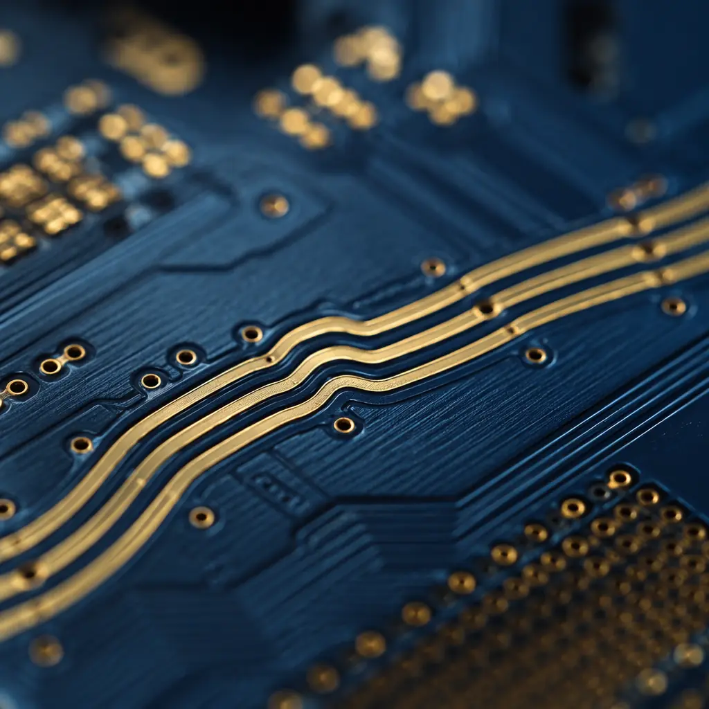
Complete PCB signal integrity design guide covering crosstalk prevention, termination strategies, differential pair routing, return path design
Upload your Gerber files and BOM. We'll respond within 24 hours with a detailed quote and free DFM review.