
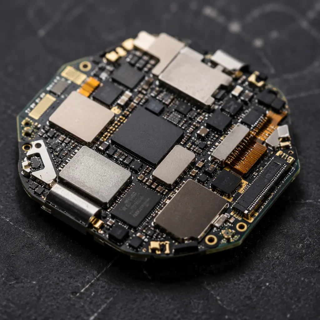
Inside a typical smartwatch, the main board measures roughly 25 × 25 mm and carries an application processor, 6-8 layers of routing, a 0.4 mm pitch BGA, a Bluetooth/Wi-Fi combo radio, a GPS receiver, an NFC antenna, a wireless charging coil input, an AMOLED display connector and a PPG heart-rate optical front end. It runs on a 300-450 mAh cell that has to survive a full day of use, and the whole assembly is sealed against 5 ATM of water. The design is a density problem first, a power problem second, and an RF coexistence problem always.
This guide covers the four disciplines that define a smartwatch board: the HDI stackup and microvia strategy, the battery and power-path design that sets real battery life, the wireless coexistence layout, and the display/sensor integration. It closes with the sealing and manufacturing steps that make a 5 ATM watch that still passes RF at final test. Huaxing PCBA assembles wearables and portable electronics across 8 SMT lines, the miniaturization rules here overlap directly with our TWS earbud boards and medical wearable boards.
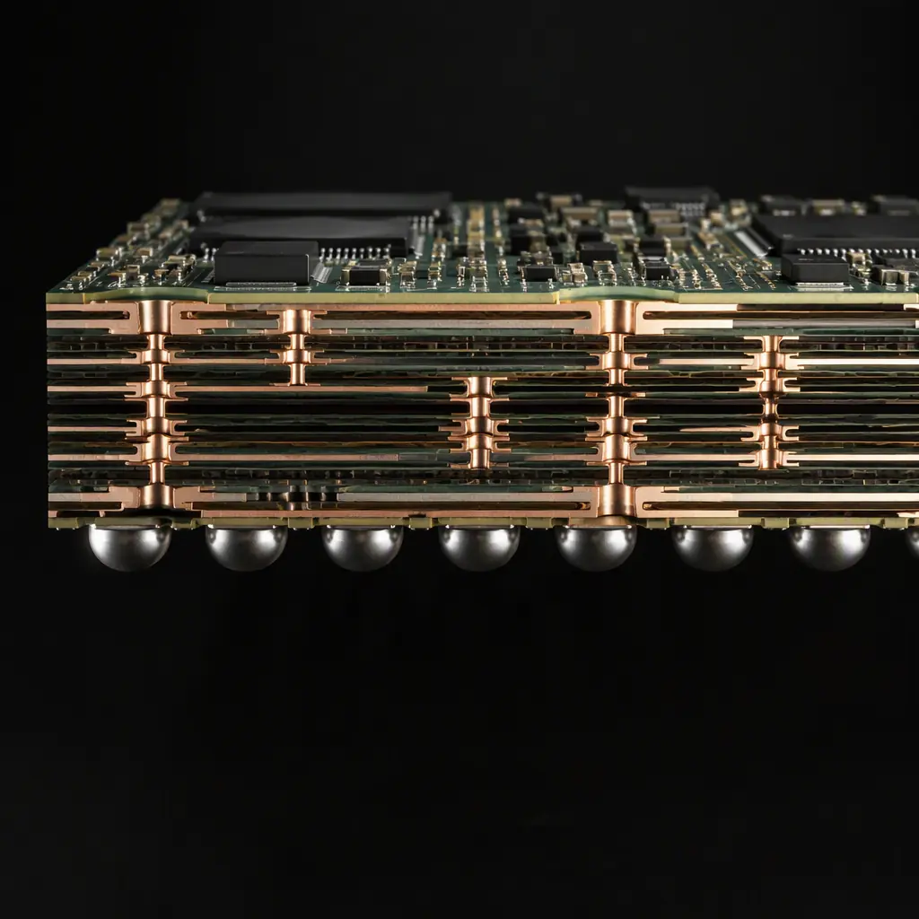
Stackup and HDI: Fitting 8 Layers into 1 mm
A smartwatch board is almost always HDI with blind and buried vias, the routing density on a 25 mm board simply cannot be achieved with through-hole vias alone. A typical construction is 6-8 layers with two or three HDI build-ups: laser microvias of 0.075–0.1 mm diameter connecting adjacent layers, buried vias in the core, and only a handful of through vias at the board edge.
Choose the HDI build-up level by BGA pitch
A 0.4 mm pitch application processor BGA needs microvias in the pads (via-in-pad) to escape the inner rows. Which means laser vias plated and filled (via-in-pad plated over, or VIPPO). 0.5 mm pitch packages can often escape with microvias beside the pads. The HDI technology guide maps BGA pitch to the right build-up level and via costs.
Keep the RF layers disciplined
With this much layer hopping, the radio sections need a defined reference: the antenna feed and the 2.4 GHz traces should sit on a layer with an unbroken ground plane beneath, with microvias stitching the ground around every RF component. The via technology guide covers the via-stitching patterns that keep RF grounds solid.
Flex-rigid for the sensor and antenna tails
Many watches use a rigid main board with a flex tail carrying the display connector, and some fold a flex antenna around the case curve. Flex-rigid construction saves two board-to-board connectors and their height budget. The flex PCB guide covers bend-radius rules and flex-rigid transition design.
Key Takeaway: The stackup is the smartwatch's real estate plan. HDI build-up level, via-in-pad for the BGA and a disciplined RF ground layer decide whether the board fits, and whether the radios work.
Battery and Power Path: Where Battery Life Is Actually Won
Marketing battery life is measured in the lab; real battery life is decided by the power-path design: how the charger, fuel gauge and DC-DC rails interact, and how much current the board leaks when the screen is off.
Power-path topology: charge and run at the same time
A linear or switch-mode charger with a power-path FET lets the watch run from the charger while charging the cell, essential because the wearer charges overnight while wearing the device for sleep tracking. The power-path MOSFET's Rdson and the charger's thermal footprint both matter in a sealed case; a 1 A charge current at 0.5 V dropout is 0.5 W of heat in a case with no airflow. The portable power design guide covers charger thermal layout.
Fuel gauge accuracy needs a clean sense path
The coulomb-counting fuel gauge measures milliohms of sense resistance; its sense traces must be Kelvin-connected directly at the battery terminals and kept away from switching noise. A poorly routed sense path adds 1-3% error, the difference between "30% at 9 pm" and "dead at 6 pm" on a 350 mAh cell.
Minimize the always-on budget
An always-on display plus continuous PPG sampling draws 300-800 µA that no marketing slide shows. The board's contribution is leakage: every pull-up resistor, every regulator's quiescent current, every rail left powered in sleep. Low-quiescent LDOs (1-3 µA) on the always-on rails and switched rails for the radio and display are board decisions with a direct battery-life payoff. The power integrity guide covers rail planning for battery products.
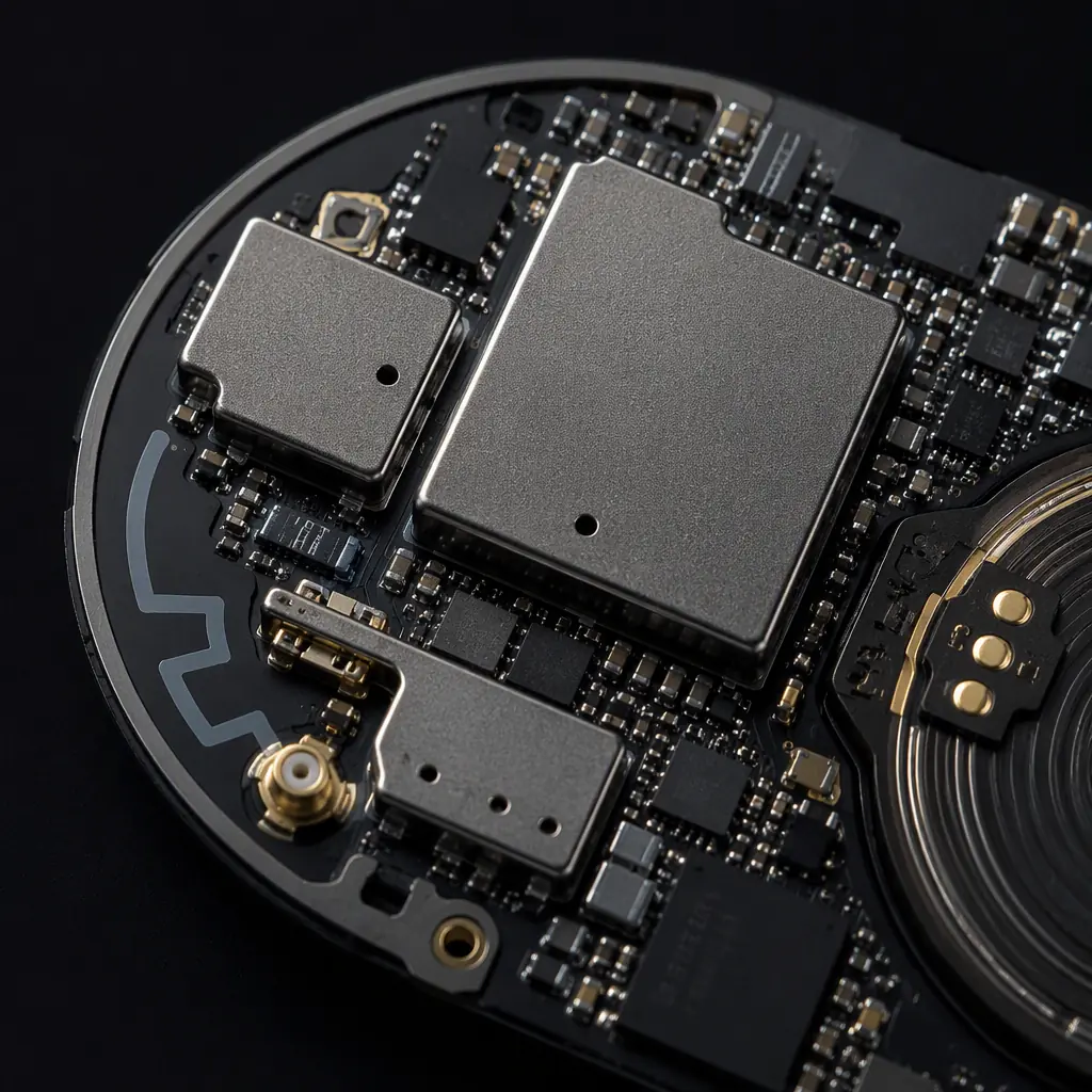
Wireless Coexistence: Four Radios in One Wrist
A modern watch runs Bluetooth Low Energy, Wi-Fi, GPS and NFC simultaneously in a metal-and-glass case with an antenna volume of a few cubic centimeters. The antennas and their grounding are the design, not an afterthought.
Antenna placement and clearance zones
The BLE/Wi-Fi antenna needs a keep-out zone clear of ground, components and the battery (which is a lossy conductor), usually at the bezel or on a flex folded against the case. The antenna feed line must be a controlled 50 Ω trace with a clean ground reference. The antenna design guide covers feed-line and clearance rules for compact devices.
Coexistence: BLE + Wi-Fi + GPS sharing the case
BLE and Wi-Fi on the same combo chip share a radio and are time-multiplexed, but GPS and NFC are separate silicon that must not be desensitized. Practical board rules: keep the GPS front end and its TCXO on a quiet corner, shield the radio sections with cans, and route the NFC antenna loop away from the switching chargers. NFC reads millivolts of coupled field at 13.56 MHz and a noisy charger kills tap-to-pay range. The BLE PCB guide and GPS receiver guide cover the layout specifics.
Wireless charging coil: keep the rectifier quiet
The wireless charging receiver coil feeds a bridge rectifier and a buck stage; the switching noise from that path couples into the battery sense and the NFC loop. The coil input, rectifier and buck should form a contained island with its own ground, tied to the system ground at one point.
Display and Sensors: AMOLED, PPG and the Analog Front End
The AMOLED panel connects over MIPI-DSI, the touch sensor over I²C, and the PPG heart-rate sensor is an optical-analog hybrid, an LED driver, photodiodes and a transimpedance amplifier reading nanowatt-level reflected light.
MIPI-DSI to the display: short, shielded, impedance-controlled
The DSI lanes (100 Ω differential) run from the processor BGA to the display FPC connector, typically on the same board or a short flex. Keep the lanes matched, away from the switching regulators, and reference them to a solid ground. The display driver guide has the DSI routing rules.
PPG optical isolation: light must not leak
The PPG LED and photodiode sit behind the watch glass with a small optical barrier between them. On the board, the LED drive traces and the photodiode amplifier traces must be kept apart, with a guard ring around the photodiode input; any LED current coupling into the amplifier reads as a false pulse. The amplifier's reference must be clean, the same discipline as our sensor board guide.
Haptics: the LRA driver is a small power stage
The linear resonant actuator (LRA) driver switches 100-200 mA at the resonant frequency (typically 150-250 Hz) and its coil is an inductor. It needs the same freewheeling and decoupling discipline as any motor driver, and its traces should not run under the PPG amplifier.
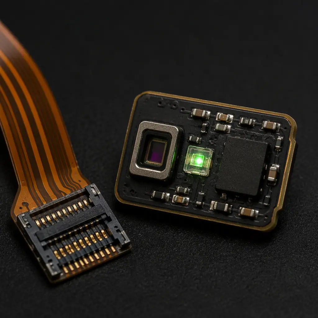
Sealing, Reliability and Manufacturing
IP68 / 5 ATM sealing changes manufacturing: the board must survive conformal coating, the battery must be potted or pocketed, and the RF still has to pass with the metal case and glass installed.
Conformal coating or selective encapsulation
The main board gets a thin conformal coating (or selective encapsulation around the BGA and connector areas), with the RF test points and battery contacts masked. The coating protects against sweat, condensation and the micro-droplets that every water-resistance test eventually admits. The conformal coating guide covers selective coating for mixed RF/analog boards.
Fine-pitch assembly and X-ray verification
0.4 mm pitch BGAs, 0201/01005 passives and microvias-in-pad push every step of the SMT process: stencil design, placement accuracy and reflow profile all matter. X-ray inspection of the BGA and the filled vias is a per-lot requirement. The fine-pitch SMT guide and inspection guide cover the process controls.
Final test with the case closed, RF first
The production test sequence runs RF (BLE/Wi-Fi/GPS/NFC) with the shield cans and case installed, antenna tuning shifts with the enclosure, then display, touch, sensors and charging. Moisture ingress testing (IPX7 dunk) runs on a sampling basis. The testing methods guide covers the station sequencing.
Building a Watch That Lasts All Day, Every Day
The design order for a smartwatch board is: the HDI stackup and via strategy first (they set the density ceiling), then the battery and power path (they set real battery life), then the radio layout with coexistence as a first-class constraint, then the display and optical front end. Seal it, coat it, and test RF with the case closed. Each discipline is a board-level decision, microvia level, power-path topology, antenna clearance, DSI routing. The watches that survive a day of wear and two years of charging are the ones whose boards were designed as tiny systems with a power budget, not as shrunk phone boards. The medical wearable guide shows how the same discipline scales to regulated health devices.
Huaxing PCBA assembles smartwatch and wearable boards with 0.4 mm pitch BGA capability, laser-microvia HDI support, selective conformal coating and case-closed RF final test across 8 SMT lines. Read our TWS earbud guide for another miniaturization case study, or send your board outline and BOM . We'll return a DFM review covering the stackup, via-in-pad and RF layout with your quote within 24 hours.
