
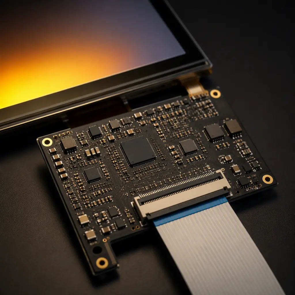
Display driver boards are the quiet workhorses of modern electronics: they sit between a processor and a display panel, converting the host's video signal into the panel's native interface, driving the backlight, and digitizing the touch layer. The design challenge is that these three functions, high-speed video, high-current backlight, and sensitive analog touch, are electrically hostile to each other and physically packed onto one board. A 1080p LVDS link runs at ~680 Mbps per lane; a backlight boost converter switches several amps; a capacitive touch controller measures femtofarad-level changes. Getting all three to coexist is the art of display driver board design.
This guide covers the three subsystems in order of electrical risk: the video interface (LVDS, eDP, MIPI-DSI) and its routing rules, the backlight driver and its EMI and thermal traps, and the touch controller integration. We manufacture display driver boards: including automotive-grade and medical-grade builds. Across 8 SMT lines in Shenzhen, and the layout rules here are the ones we verify in every DFM review. Start with our signal integrity guide if you need the differential-pair fundamentals first.
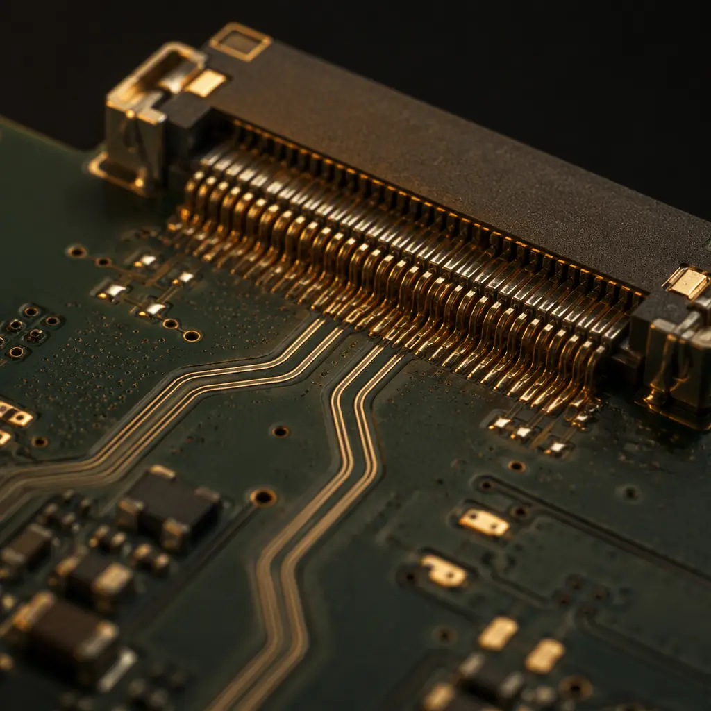
Choosing the Panel Interface: LVDS vs eDP vs MIPI-DSI
The interface choice is usually dictated by the panel and the SoC, but each has distinct PCB design implications:
| Interface | Typical Use | Speed per Lane | PCB Impact |
|---|---|---|---|
| LVDS (FPD-Link) | Industrial, medical, older automotive | ~680 Mbps (1080p) | 4-8 pairs, 100 Ω differential, forgiving but bulky |
| eDP | Laptops, tablets, modern monitors | 1.62-8.1 Gbps (HBR1-HBR3) | High-loss concern, short stubs, impedance at panel spec |
| MIPI-DSI | Smartphones, tablets, embedded Linux | up to 2.5 Gbps/lane | Differential 100 Ω, tight skew, often on flex or short traces |
| RGB parallel | Small TFTs, legacy MCU systems | 25-100 MHz parallel | Routing length matching across 16-24 data lines |
LVDS remains the workhorse for industrial and automotive displays because of its noise immunity and long-cable tolerance; eDP is taking over where bandwidth demands grow. Whatever the interface, the routing rules below are the same: controlled impedance, matched skew, and a clean reference plane. For HDMI and DisplayPort, the source side of many driver boards, see our HDMI/DisplayPort design guide.
Differential Pair Routing Rules That Actually Matter
High-speed video routing fails in predictable ways, and the fixes are well known. The top five rules, in order of impact:
Controlled impedance with the right stackup
LVDS pairs need 100 Ω differential impedance; eDP and MIPI-DSI too. That requires a stackup with tightly controlled dielectric thickness: typically a 4-8 layer board with the signal layers adjacent to solid reference planes. Do not rely on "close enough" stackups from a cheap fab; specify the impedance and get a TDR report with the boards. Our stackup design guide walks through the layer math.
Intra-pair skew under 5-10 mils
Within a pair, the P and N traces must be length-matched to within a few mils. At 680 Mbps, 10 mils of skew is roughly 1% of a bit period, which is tolerable, but at eDP HBR2 speeds the budget shrinks dramatically. Route pairs tightly together and add serpentine compensation at the source. Skew between pairs (channel-to-channel) matters less but should stay under ~50 mils.
Continuous reference plane, no splits under pairs
The return current of a differential pair flows in the reference plane directly beneath it. A split or gap in that plane forces the return current to detour, creating loop inductance and common-mode noise. If a plane must split, route pairs around the split, never across it. This is also the first thing a CM's DFM check looks for when a display board fails EMC.
Via discipline: matched via counts and no stubs
Every via on a high-speed pair adds capacitance and inductance. Use the same via count and via size for both traces in a pair, and back-drill or avoid long via stubs on eDP above HBR1. On MIPI-DSI routed to a board-to-board connector, keep the total stub under the panel's spec: often 10 mils or less for 2.5 Gbps lanes.
Route video away from the backlight switcher
The backlight boost converter is the noisiest thing on the board. Keep the video differential pairs physically separated from the switcher's input/output loops, and never run them parallel to the backlight LED return path. If space forces proximity, use a ground guard trace between the video bundle and the switcher. Our crosstalk analysis guide quantifies the coupling you are trying to avoid.
Key Takeaway: Impedance and reference-plane integrity account for 80% of video-interface failures. Get the stackup right and keep the planes solid, and most other routing sins become survivable.
Backlight Driver Design: Boost Converter, LED String, and PWM Dimming
The backlight subsystem is where display driver boards fail in the field: usually from heat or EMI. The backlight LED string typically needs 20-40 V from a 5-12 V input, which means a boost converter. Design decisions that matter:
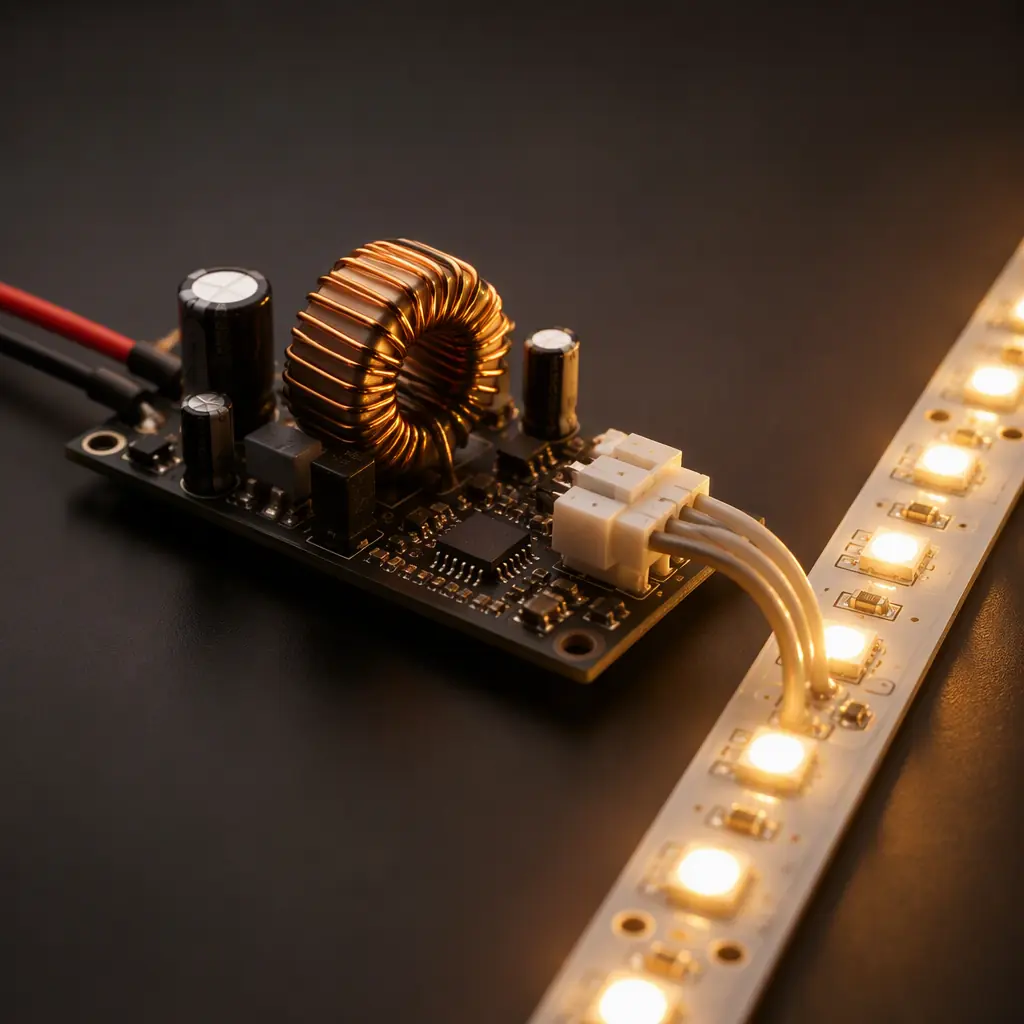
Size the inductor and switching loop for the string voltage
A boost converter's inductor stores the energy that gets dumped into the LED string. The switching node (FET drain, inductor, diode) must be a tight loop with low inductance. A large loop here is the #1 cause of radiated EMI on display boards. Follow the layout in the driver IC's datasheet literally; the pinout is designed around loop area. Our power integrity guide covers the loop-area analysis in depth.
Plan the heat path for the LED driver and inductor
At 3-5 A output and 90% efficiency, the backlight chain dissipates 1-3 W across the FET, diode, and inductor. On a sealed display, that heat must spread into the board copper and out to the housing. Use wide copper pours, thermal vias under the driver IC, and keep the inductor's heat away from the video connector and touch controller. See our thermal management guide for the via arrays and copper budgeting.
PWM dimming: keep the frequency out of the audible and touch ranges
PWM dimming at 200 Hz-1 kHz is standard, but the switching transient can couple into the touch controller and produce jitter or false touches. Options: use a dimming frequency above the touch scan rate (or below it), add a small RC filter on the touch supply, or use analog/DC dimming for the last 10% of brightness. The touch controller's datasheet usually specifies the exact frequencies to avoid.
Protect the LED string and connector
Add OVP (over-voltage protection) on the boost output, a soft-start to limit inrush, and TVS/filtering on the backlight connector pins. LED string failures, an open LED, can otherwise take out the whole driver. For the protection component choices, our ESD protection guide has the selection criteria.
Touch Controller Integration: The Noise-Sensitive Analog
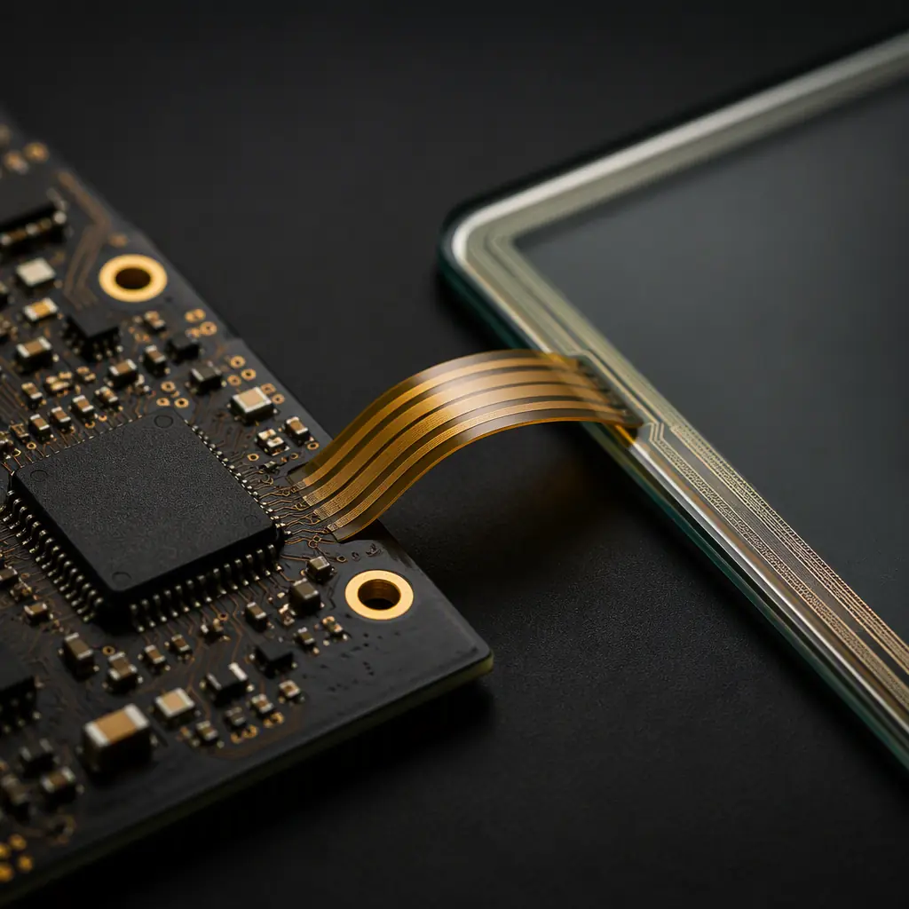
Capacitive touch controllers measure tiny capacitance changes on the sensor electrodes. And every switching signal on the board is a potential interferer. Integration rules:
Dedicated, filtered supply for the touch IC
Give the touch controller its own LDO or filtered rail, not a direct tap off the main 3.3 V that also feeds the video serializer. A ferrite bead plus 1-10 µF bypass on the touch supply removes most conducted noise. Keep the touch IC's ground return separate from the backlight return all the way to the input connector.
Route the flex/sensor connection as a guarded bundle
The traces from the touch controller to the sensor (often over a flex cable or an FPC connector) carry the weakest signals on the board. Route them as a tight group with a ground guard, away from the video pairs and the backlight output. Length matching within the group matters less than isolation from noise sources.
Ground the display frame and connector shields
The panel's metal frame and the FPC connector's ground shield must connect solidly to the board ground, a floating frame becomes an antenna that couples noise straight into the touch electrodes. Use multiple stitching vias around the connector footprint.
For touchscreens that must pass ESD testing (IEC 61000-4-2), the touch traces' entry point at the connector needs TVS clamps before the controller, see our ESD packaging and handling guide for the full protection strategy across the assembly lifecycle.
Manufacturing Notes for Display Driver Boards
Display driver boards have manufacturing quirks that a good CM will flag in DFM:
| Issue | Why It Happens | What to Specify |
|---|---|---|
| Impedance drift on outer layers | Solder mask changes effective dielectric constant | Specify impedance with solder mask; request TDR coupons per panel |
| FPC connector solder defects | Fine-pitch (0.3-0.5 mm) connectors, paste misregistration | Laser-cut stencil, X-ray inspection on connector joints |
| Board warp with backlight copper | Uneven copper distribution (heavy pours on one side) | Balanced stackup, cross-hatched pours if needed, panelization strategy |
| Touch flex soldering | Heat damage to flex tail during reflow | Sequential or hand-solder step, thermal profile validation |
| Cleanliness for high-impedance nodes | Flux residue on touch sensing circuits | Aqueous cleaning or no-clean flux validated for impedance |
If your display driver board feeds a medical monitor or automotive display, add the relevant reliability testing, thermal cycling and vibration for automotive (see our thermal cycling guide), and the longer-term stability testing medical requires. For high-volume builds, our testing methods guide covers ICT and functional test strategies that catch display faults before shipping.
Summary: Display Driver Board Design Checklist
| Subsystem | Checklist Item |
|---|---|
| Video interface | 100 Ω controlled impedance; intra-pair skew <10 mils; continuous reference planes; matched vias; no stubs on eDP HBR2+ |
| Backlight | Tight boost switching loop; OVP + soft-start; heat path sized for 1-3 W; dimming frequency clear of touch scan rate |
| Touch | Dedicated filtered supply; guarded sensor routing; grounded frame and connector shields; TVS at connector entry |
| Manufacturing | TDR impedance verification; X-ray on fine-pitch connectors; balanced copper for warp control; validated cleaning process |
At Huaxing PCBA, we build display driver boards from prototype to high-volume, with impedance-controlled stackups, X-ray inspection on fine-pitch connectors, and DFM review that checks exactly the rules in this guide. If you are designing a display driver board, for a car, a medical device, or an industrial HMI, send us your design files and we will return a DFM report within 24 hours. Contact our engineering team, or read our FPGA PCB design guide if your driver board is FPGA-based.
