
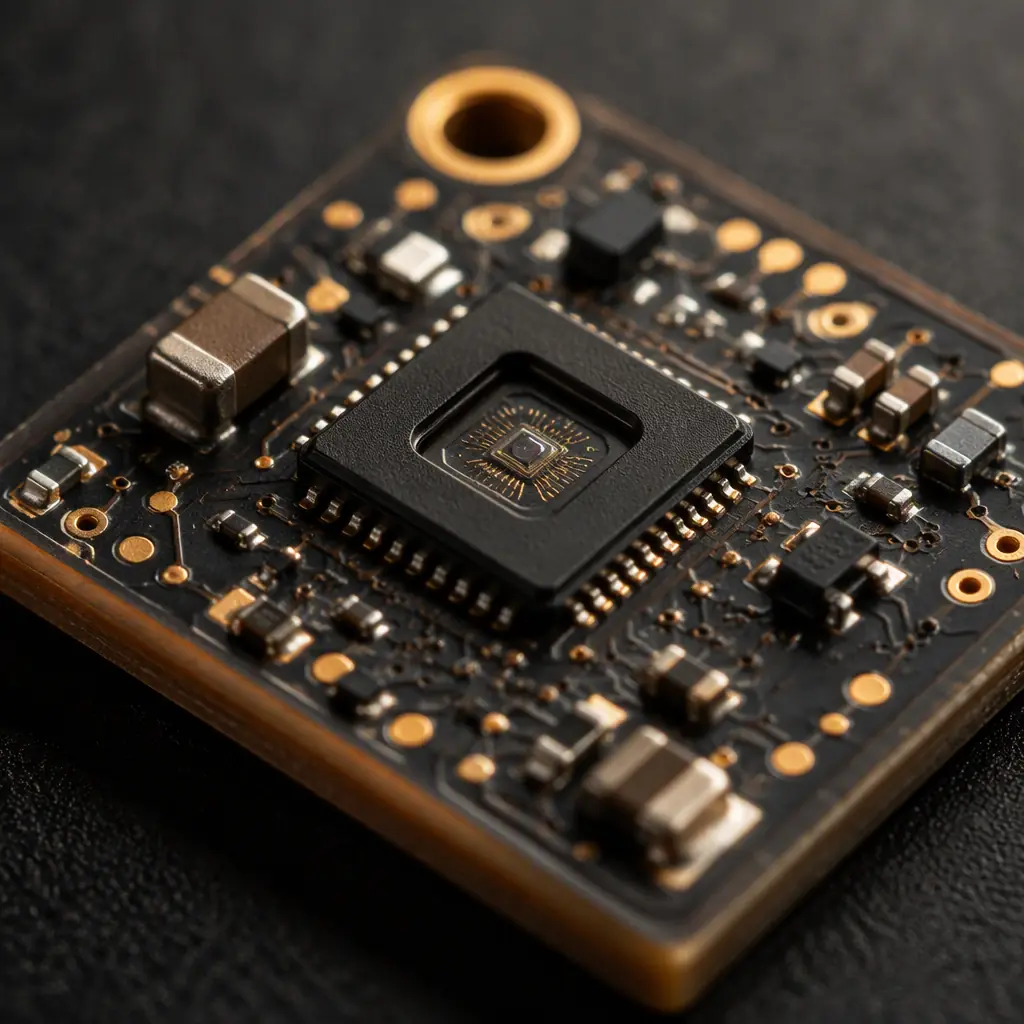
MEMS sensors — accelerometers, gyroscopes, magnetometers, pressure sensors, and microphones — are the smallest precision instruments in modern electronics. They are also uniquely sensitive to their environment: the same PCB that carries power and data can inject mechanical stress, thermal drift, and electrical noise into the measurement. A design that ignores the sensor's physical needs produces drift and bias errors no amount of firmware calibration can fully remove.
Huaxing PCBA assembles MEMS sensor modules for industrial and IoT customers — vibration monitoring, tilt sensing, and environmental sensing boards — with the controlled reflow profiles and X-ray inspection that small-package sensors require. This guide covers package selection, land patterns, grounding, mechanical stress isolation, and the assembly practices that keep a MEMS device accurate after thousands of hours. For the wider IoT context, see our IoT PCB design guide.
How MEMS Packages Differ from Ordinary ICs
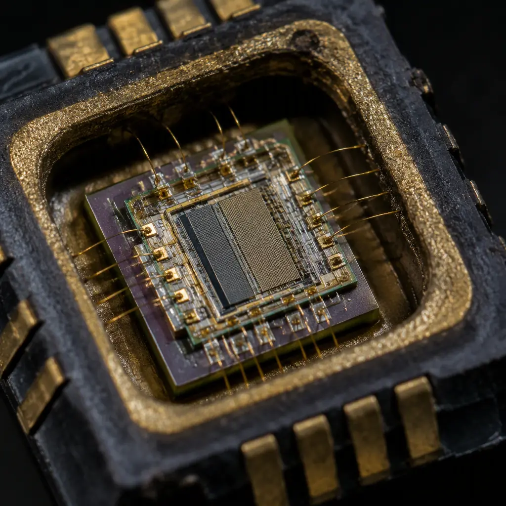
A MEMS device is a moving part sealed inside a package: a proof mass suspended on silicon springs, a diaphragm, or a resonating beam. That mechanical core makes the package different from a standard IC in three ways that affect the board design.
| Property | Standard IC | MEMS Sensor |
|---|---|---|
| Mechanical sensitivity | None | Measures acceleration / pressure / rotation |
| Package cavity | Solid mold | Often a cavity or open window (pressure, microphone) |
| Stress sensitivity | Low | High — PCB strain shifts offset |
| Reflow sensitivity | Standard | Moisture + thermal profile critical |
| Placement constraint | None | Location, orientation, and nearby mass matter |
The mechanical coupling between the package and the board is the core problem. When the board bends — from vibration, thermal expansion, or a nearby screw — that strain transfers into the package and shifts the sensor's zero-g offset. The layout job is to decouple the sensor from board strain. Our thermal management guide covers the board-level mechanics that interact with this.
Land Patterns and Placement: Give the Sensor a Quiet Corner
Sensor placement is a mechanical decision, not just a routing one. The device should sit on a stiff part of the board, away from mounting holes, board edges, and large components that create localized bending. A sensor near a corner screw sees the full panel strain; one at the center of a stiff panel sees very little.
Follow the Vendor Land Pattern Exactly
MEMS packages are sensitive to solder volume under the die. Use the vendor-recommended land pattern and stencil apertures — do not widen pads for "better" wetting. Asymmetric solder joints under a MEMS die create bias shifts. Our stencil design guide covers aperture sizing for small packages.
Keep the Sensor Axis and Datum Clear
For inertial sensors, the reference edge and axis orientation must be unambiguous on the assembly drawing. A 90° rotation error in placement is a silent field failure. Mark the axis on the silkscreen and confirm orientation in the pick-and-place program review.
Leave Room for the Decoupling Caps
The sensor's supply pin needs a 0.1 µF capacitor as close as physically possible, plus a bulk cap within a few millimeters. The cap placement affects the noise floor more than the sensor's own datasheet number in many designs. Our power integrity guide explains the decoupling rules.

Grounding and Analog Front-End Discipline
MEMS sensors output small analog signals — often in the microvolt range before amplification. The analog front end (amplifier, ADC) must be protected from the digital noise on the same board: switching regulators, digital buses, and RF all couple into high-impedance sensor traces.
Use One Solid Ground Plane, Not Split Analog/Digital
Modern mixed-signal practice is a single continuous ground plane with the analog circuitry grouped in one region. Splitting the plane creates return-path discontinuities that radiate and couple. Our mixed-signal design guide details the single-plane methodology.
Keep Sensor Traces Short and Guarded
Route the sensor output to the amplifier with the shortest possible trace, and consider a ground guard trace around the analog section. Keep high-speed digital routes off the layers adjacent to the sensor's sensitive nets. The crosstalk analysis guide quantifies the coupling budget.
Filter the Supply, Not Just the Output
A ferrite bead plus 10 µF and 0.1 µF on the sensor supply cleans the rail better than any output filter. Switching regulator ripple at 100–500 kHz rides straight through an unfiltered supply into the measurement. Our PDN design guide covers supply filtering in depth.
Mechanical Stress Isolation: The Rule Most Layouts Miss
Board strain is the number one cause of MEMS offset drift in real products. The fix is structural, and it has to be designed in at layout time:
Move the Sensor Away from Mounting Points
Keep a minimum of 5–10 mm between the sensor and any mounting hole, connector, or standoff. That distance lets the board flex absorb strain before it reaches the package.
Consider a Soft-Mount or Isolated Sub-Board
For high-vibration applications, mount the sensor on a small sub-board connected through compliant pins or a flex tail. This mechanically decouples the sensing element from the main board's resonance. Our flex PCB guide covers the dynamic-flex design rules for such tails.
Avoid Copper Pours Under the Package That Tear
Large unbroken copper under a MEMS package can amplify thermal stress during reflow. Follow the vendor's recommendation — typically a solid pad or a specific tie pattern, not a full pour with random thermal spokes. Our warpage prevention guide covers the thermal-stress side.
Key Takeaway: If the sensor drifts more than the datasheet allows, suspect the board before the sensor. Placement near mounting hardware, split grounds, and unfiltered supplies cause more MEMS field failures than the devices themselves.
Assembly: Reflow, Moisture, and Inspection
MEMS packages carry the same moisture-sensitivity and reflow requirements as other small packages — plus a few of their own. The cavity and the moving structure mean solder paste, flux, and handling all matter more.
Respect the Moisture Sensitivity Level
Many MEMS packages are MSL 3 or tighter. If the floor life is exceeded, the trapped moisture can delaminate the cavity during reflow. Our MSL guide covers baking and handling requirements.
Hold the Reflow Profile Inside the Window
Use the sensor vendor's peak-temperature and time-above-liquidus limits, which are often tighter than the general IPC profile. A profile that works for the rest of the board may violate the sensor's window. Our reflow profile guide explains the optimization process.
No-Clean Flux Verification for Cavity Packages
Flux residue under a cavity package can migrate and corrode bond wires over time. Verify the no-clean residue is compatible with the package, or plan a cleaning step. The PCB cleaning guide compares aqueous and solvent options.
X-Ray the First Article
Confirm solder coverage under the package and check for voids in the die-attach region. Voids under a MEMS die change the thermal and mechanical path and shift calibration. Our AOI/X-ray/SPI guide lists the inspection recipes.

Testing: Calibrate on the Board, Not Just the Bench
A MEMS sensor is calibrated at the factory, but board assembly adds its own offset: solder stress, component placement, and board curvature all shift the zero point. Production testing should capture and compensate for the board-level contribution.
Run a Board-Level Zero-G / Zero-Pressure Check
Measure the sensor output in a known orientation at final test and store the offset in the product's calibration memory. This catches assembly-induced drift before the unit ships. Our testing methods guide covers the full test strategy.
Thermal-Cycle a Sample for Offset Stability
Board stress relaxes over thermal cycles, shifting the offset. Cycling a sample through −40°C to +85°C and re-measuring quantifies the drift your product will see. The thermal cycling guide describes the test methods.
Summary: Treat the Sensor as a Precision Instrument
A MEMS sensor board succeeds when the PCB behaves like a stable platform: stiff where the sensor sits, quiet on the analog side, and free of strain coupling from mounting and assembly. The rules are concrete — vendor land patterns, single-plane grounding, filtered supplies, placement away from hardware, controlled reflow, and board-level calibration.
At Huaxing PCBA, we assemble MEMS sensor modules with controlled reflow, X-ray inspection, and functional test support, from prototypes to production volumes. Read our IoT PCB guide for the surrounding system design, or send your sensor layout for a DFM review focused on the mechanical and assembly risks before you commit to tooling.
