
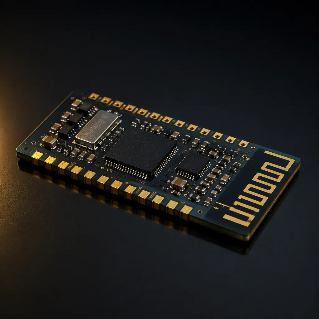
Bluetooth Low Energy is the default wireless link for billions of battery-powered devices — wearables, beacons, medical sensors, smart locks, and industrial IoT nodes ship in the tens of millions per quarter. But BLE is also unforgiving: the entire radio operates in the 2.4 GHz ISM band with a sensitivity budget of roughly -96 dBm, which means a poorly laid-out antenna or a noisy power rail can cost you 10-20 dB of link margin before the firmware ever runs.
Huaxing PCBA manufactures BLE modules and host boards for IoT brands worldwide — controlled-impedance stackups to 50 Ω on the RF path, chip and PCB trace antenna designs with matching networks, and 100% RF-tested boards with conducted and radiated measurements on every lot. This guide covers the layout decisions that determine real-world range, the matching and crystal rules that keep production yields high, and the testing you should demand from your manufacturer.
Why BLE Layout Is Different From a Digital Board
BLE operates in the 2.4-2.4835 GHz ISM band with 40 channels of 2 MHz spacing — 37 data channels and 3 advertising channels. At 2.4 GHz the wavelength is 125 mm, so a quarter-wave antenna is only 31 mm, and every millimeter of trace, every via, and every ground gap on the RF path becomes electrically significant. The same rules that would be harmless on a 100 MHz digital bus can detune a BLE antenna by tens of MHz.
| BLE Feature | Value | PCB Design Impact |
|---|---|---|
| Frequency band | 2.400-2.4835 GHz | Quarter-wave antenna ≈ 31 mm; trace length matters |
| Channel spacing | 2 MHz (40 channels) | Sharp tuning; ±2-3 MHz detune hurts adjacent channels |
| Data rates (BLE 5.x) | 125 kbps - 2 Mbps | Coded PHY gives range; 2 Mbps needs clean RF path |
| TX power | 0 dBm typical (up to +8 dBm) | Regulatory limit 10 dBm EIRP; antenna gain must be checked |
| RX sensitivity | -96 dBm typical | Noise on power rails directly steals sensitivity |
| Crystal tolerance | ±20 ppm typical (BLE spec ±50 ppm total) | Load capacitance tuning on the crystal pins |
The practical consequence: a BLE board needs a controlled-impedance RF section, a clean ground reference under the antenna feed, and decoupling discipline that a purely digital board never demands. Our impedance control guide explains how to specify the 50 Ω targets on your fabrication drawing, and the RF PCB guide covers the material and stackup choices for 2.4 GHz work.
Antenna Design: Trace, Chip, or Module-Mounted?
Every BLE product must pick an antenna strategy, and the choice drives the entire RF layout. There are three common options, each with different PCB real estate, cost, and tuning requirements.
PCB Trace Antenna (Inverted-F / Meander)
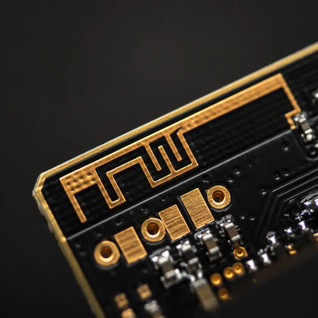
A printed inverted-F antenna (IFA) on the board edge costs nothing in BOM and is the most common choice for high-volume BLE products. The classic IFA occupies roughly 25 × 8 mm on a 1.6 mm FR-4 board, with a ground clearance of 2-3 mm around it and a feed point that connects through a π matching network to the radio. Performance depends on the ground plane underneath being continuous — cut it for battery or antenna keep-out and the resonant frequency shifts. Our stackup design guide shows how to allocate the RF layer in a multilayer board.
Chip Antenna (Ceramic)
A ceramic chip antenna (for example, 3.2 × 1.6 mm or 1.6 × 0.8 mm) takes far less board area than a trace antenna and is less sensitive to enclosure effects, which makes it the default for wearables and small IoT nodes. The trade-off is a narrower bandwidth and stricter layout rules — the datasheet's ground clearance, keep-out, and matching values must be followed almost exactly, and the antenna needs its own clear ground zone with no traces underneath. Our antenna PCB guide covers the grounding discipline for small antennas.
Pre-Certified Module (Chip + Antenna On Board)
Using a pre-certified BLE module (FCC/CE module grants) moves the antenna design burden to the module vendor. Your PCB then only needs to follow the module's recommended footprint — usually a ground keep-out under the antenna and a clean area around it. This is the fastest path to market and the safest for low-volume products, at a per-unit cost premium of roughly $1-3. For volume above 50-100k units/year, most brands move to a custom trace or chip antenna design to save BOM cost.
Key Takeaway: Whatever antenna you choose, the ground plane directly beneath it is part of the antenna. A keep-out that is too small, a split ground, or a battery that sits under the antenna zone will detune the design regardless of how well the matching network is tuned. Decide the antenna zone first, then route everything else around it.
The 50 Ω Feed and the π Matching Network
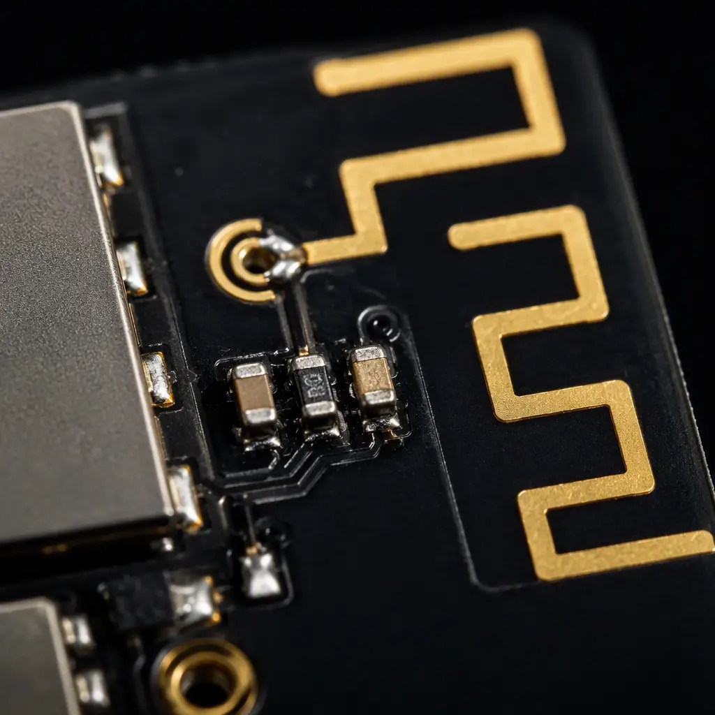
Between the BLE SoC's RF pin and the antenna sits a controlled-impedance trace and a matching network, typically a π or L configuration of two to three components. This network tunes out the impedance mismatch between the radio output and the antenna, and it is the most common source of RF yield loss in production.
Keep the RF Trace Short, Straight, and 50 Ω
The trace from the SoC RF pin to the matching network, and from the network to the antenna feed, should be a coplanar waveguide or microstrip with a controlled 50 Ω impedance. Keep the total length under 15-20 mm, avoid vias on the RF path (each via adds inductance and loss), and never route the RF trace over a split ground. Specify the impedance target on the fabrication drawing — a 10% impedance error changes return loss by about 1 dB and detunes the matching.
Use 0402 or 0201 Components With Known Parasitics
Matching components must be the size the layout was simulated with — swapping a 0402 inductor for a 0603 of the same nominal value changes the parasitic capacitance enough to shift the resonant frequency by several MHz. Specify the component sizes on the BOM and lock them with the manufacturer. The network values themselves (typically 0.5-3 nH inductors and 0.5-2 pF capacitors) are tuned during the initial board bring-up using a VNA, then fixed for production.
Ground the Shield Can Properly
If the BLE section uses an RF shield can, the can's perimeter must stitch to the ground plane with vias every 2-3 mm, and the can must not touch any component pads or traces. A poorly grounded shield can becomes a parasitic antenna element that couples noise into the RX path — a classic cause of sensitivity that looks fine in the lab but fails in the field. Our EMC compliance guide covers shield can design in the emissions context.
Crystal, Power, and Decoupling: The Quiet Support System
A BLE radio's frequency accuracy depends on a 32 MHz (or 26 MHz) crystal, and its sensitivity depends on clean supply rails. These two support systems cause more field failures than the antenna itself.
Crystal Load Capacitance: The ±20 ppm Budget
The BLE specification requires the radio to stay within ±50 ppm total frequency error, and most designs budget ±20 ppm for the crystal itself, leaving the rest for temperature drift and production tolerance. The two load capacitors on the crystal (typically 8-12 pF each, matching the crystal's specified load capacitance) must be placed close to the crystal with short traces, and the crystal must sit away from switching regulators and high-current traces. A crystal that is 30 ppm off shifts the RF channels enough to reduce sensitivity by 3-6 dB at the band edges.
Power Rail Noise Directly Steals Sensitivity
The BLE SoC's supply rails — usually a 3.3 V or 1.8 V rail from a DC-DC converter plus an internal LDO — must be decoupled with the exact capacitor values and placement from the SoC datasheet. Switching regulator ripple above roughly 20 mVpp couples into the RF front end and raises the noise floor. Place the DC-DC converter on the opposite side of the board from the RF section, or at minimum behind a ground stitch and a ferrite bead on the supply trace. Our power integrity guide has the decoupling and plane design rules.
Coexistence With Wi-Fi: Plan the PTA Lines
Most IoT products pair BLE with Wi-Fi on the same device (a smart lock, a speaker, a hub). Both radios share the 2.4 GHz band, and without coexistence management they desensitize each other. Modern designs use the 3-wire PTA (Packet Traffic Arbitration) interface between the Wi-Fi and BLE radios, plus a shared antenna or a diplexer. The PTA lines are slow control signals, but they must be routed cleanly and the antenna sharing network must be specified — this is a layout decision, not a firmware one. Our Wi-Fi PCB design guide covers the 2.4 GHz coexistence layout in detail.
Range, Link Budget, and Real-World Expectations
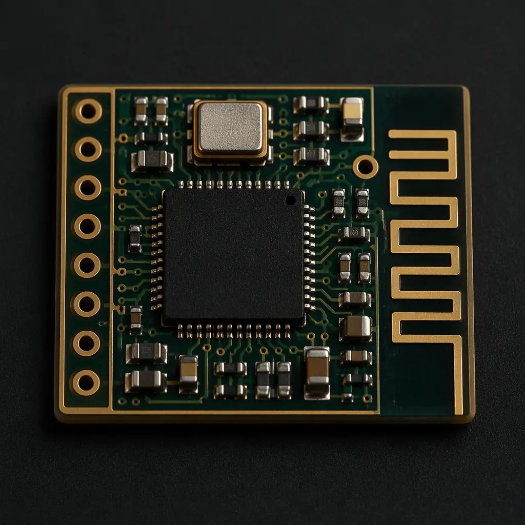
Buyers often ask "how far does BLE reach?" — the honest answer is that range is a link budget calculation, and the PCB determines several terms of that budget. A typical BLE link at 0 dBm TX power and -96 dBm sensitivity has a free-space path loss budget of about 96 dB, which maps to roughly 60-100 meters outdoors at 2.4 GHz. Indoors, walls and reflections consume 10-30 dB, dropping reliable range to 10-30 meters. Every dB lost in the PCB — antenna detuning, impedance mismatch, power rail noise — comes directly out of that budget.
| Link Budget Term | Typical Value | What Can Go Wrong on the PCB |
|---|---|---|
| TX power | 0 dBm (1 mW) | Mismatch loss at antenna feed (up to 2-3 dB) |
| Antenna gain | 0-2 dBi (trace/chip) | Detuned antenna → negative gain at band edges |
| RX sensitivity | -96 dBm | Supply noise, shield can coupling, crystal offset |
| Path loss (outdoor) | ~96 dB at 100 m | — |
| Path loss (indoor) | 70-86 dB at 10-30 m | Enclosure, battery, metal objects near antenna |
If your product must hit a specific range target — a smart lock that must reach the phone from the hallway, a beacon that must cover a warehouse aisle — state it as a link budget requirement to your manufacturer, not as "good range". The DFM review should verify the antenna zone, the impedance targets, and the matching component sizes before tooling. Our IoT PCB design guide walks through the full system-level checklist for connected products.
RF Testing You Should Demand From Your Manufacturer
BLE modules fail in production for reasons that a continuity test can never catch: a slightly detuned matching network, a ground gap under the antenna, a crystal that drifted in reflow. The only way to catch these is RF testing, and the level of testing your manufacturer offers is a direct indicator of whether they understand wireless hardware at all.
Conducted Testing: TX Power, Frequency Error, and RX Sensitivity
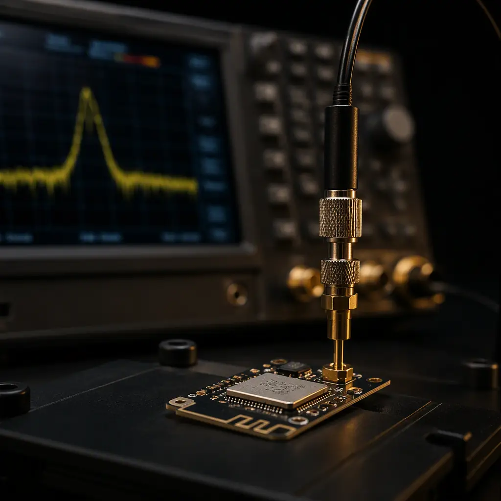
Every production board should be tested conducted — the radio's RF pin connected through a test port to a spectrum analyzer or a BLE tester. Measure TX power (should be within ±1 dB of target), carrier frequency error (within ±50 ppm, ideally ±20 ppm), and ideally RX sensitivity. A test port with a known insertion loss must be designed into the board from day one; adding it later means a board re-spin. Frequency error measurement is the cheapest way to catch crystal and reflow issues on 100% of boards.
Radiated Testing: TRP and TIS on a Sample Basis
Conducted testing verifies the radio; radiated testing verifies the antenna. Measure Total Radiated Power (TRP) and Total Isotropic Sensitivity (TIS) on a sample from each lot — typically 5-10 boards per lot in a shielded chamber. TRP should be within 1-2 dB of the design target; a 3 dB drop from one lot to the next means something changed in the PCB fab, the antenna, or the assembly. This is the test that catches silent antenna detuning. Our inspection methods guide covers how RF testing fits into the broader test strategy.
Antenna Tuning During Bring-Up: Use a VNA, Not Trial and Error
During prototype bring-up, the matching network should be tuned with a Vector Network Analyzer measuring return loss (S11) at the antenna feed. Target return loss better than -10 dB across the full 2.400-2.4835 GHz band, ideally -12 dB or better. Trial-and-error tuning without measurement routinely produces boards that work in the lab and fail certification. If your manufacturer offers VNA-based tuning and re-verification as a service, that is the single strongest signal that they ship RF hardware regularly.
Manufacturing Controls for RF Boards
RF boards fail the DFM review more often than digital boards because the layout constraints are tighter. When you send a BLE design to manufacturing, the review should specifically verify the items below — most contract manufacturers will catch gross errors, but the RF-specific ones are frequently missed.
Impedance Coupons and Verification Per Panel
Controlled-impedance boards need impedance test coupons on every panel, with the measured values reported against the ±10% (or tighter) target. Verify the target impedance is actually specified on the fab drawing — the single most common RF DFM error is a drawing that says nothing about impedance while the layout assumed 50 Ω. Our manufacturing tolerances guide covers what impedance control really costs and how to verify it.
Soldermask Over the Antenna Zone
Soldermask has a dielectric constant around 3.5-4 and adds loss and detuning when it covers the antenna and the RF trace. Specify the antenna zone and RF traces as copper-exposed (soldermask removed) or with the mask defined in the fab drawing. This is a small detail that consistently improves radiated performance by 0.5-1.5 dB. Our solder mask guide explains the material options.
Component Placement and Solder Paste for 0201 Matching Parts
0201 matching components need precise stencil apertures and placement accuracy (typically ±0.05 mm placement). Specify an SMT process qualified for 0201 — most high-volume lines handle it, but a line set up for 0402-and-larger will struggle with tombstoning and paste voids on 0201s. Our stencil design guide covers aperture design for fine-pitch and small passives.
Summary: The BLE Board Checklist
A BLE board that connects reliably treats the antenna zone as sacred space, keeps the RF feed short and at 50 Ω, tunes the matching network with a VNA during bring-up, gives the crystal and the power rails the quiet they need, plans coexistence with Wi-Fi in the layout, and verifies every board with conducted RF testing plus lot-sample radiated testing. None of it is exotic — it is disciplined RF layout backed by manufacturing controls that match the technology.
At Huaxing PCBA we manufacture BLE modules and host boards with controlled-impedance stackups, 0201-capable SMT lines, VNA-based antenna tuning support, and conducted RF test on 100% of boards with TRP/TIS radiated verification per lot. Our DFM review checks the antenna zone, impedance targets, matching component sizes, crystal placement, and RF test port design before tooling. Read our IoT PCB guide to prepare your design, or send your files for a free DFM review and quote.
