
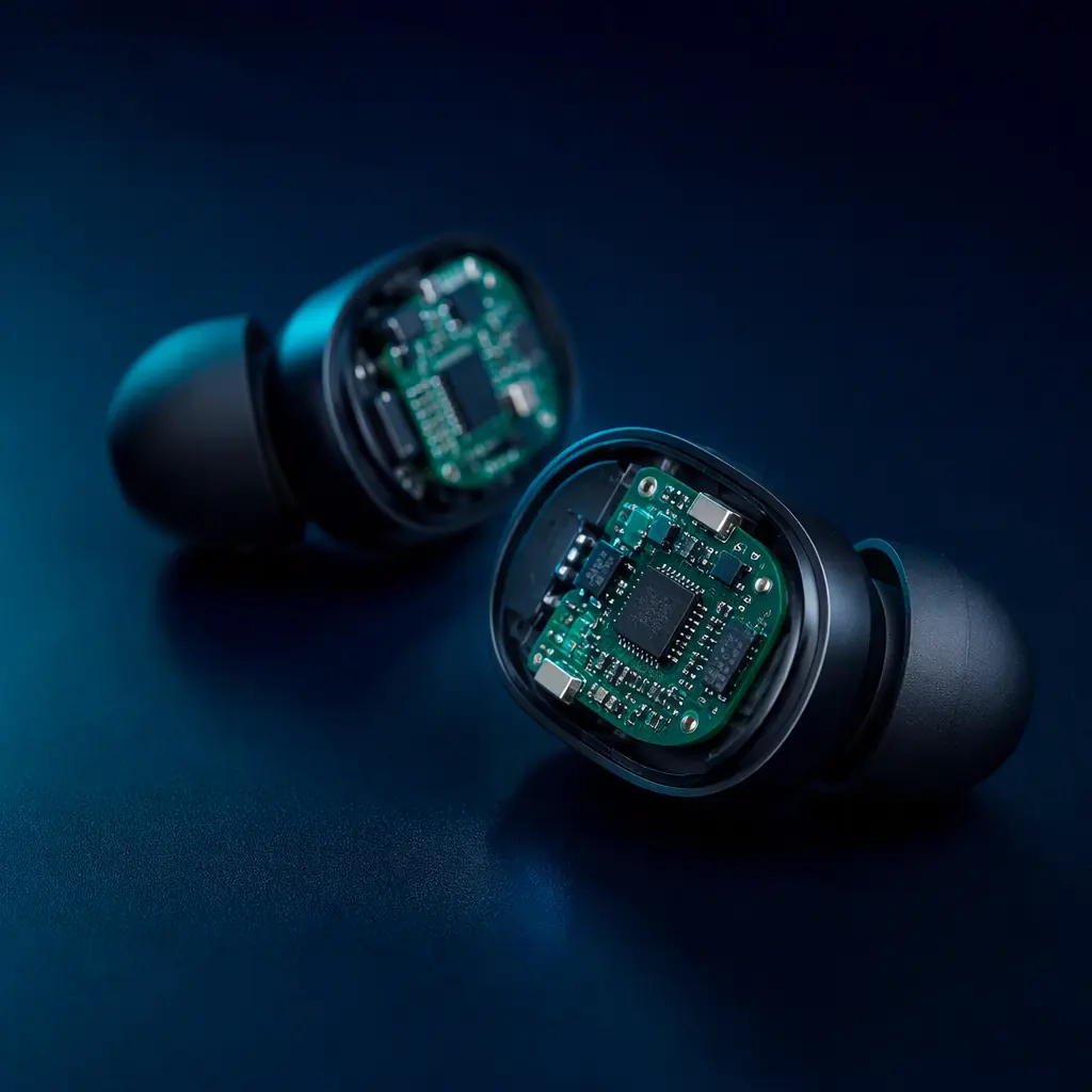
The TWS (True Wireless Stereo) earbud is one of the most demanding PCB design challenges in consumer electronics. A typical board measures just 8 × 12 mm with 4 to 6 layers, yet it must contain a 2.4 GHz radio that holds a stable link through a human head, an audio path clean enough for Hi-Res playback, microphones that reject wind noise, and a charging circuit that never shorts a lithium cell. Get any one of these wrong and the product fails in the field, not in the lab, but in the customer's ear.
This guide covers the layout rules that matter at production scale: RF and antenna placement, ANC microphone routing, charging case power design, battery protection, and the DFM constraints that determine whether a Shenzhen CM can assemble your boards at high yield. We write from the factory side: Huaxing PCBA runs 8 SMT lines with 0201 and 0.3 mm-pitch BGA capability, and we assemble millions of small-form-factor boards a year, including including hearing aids and wearables. For the fundamentals of radio layout, start with our Bluetooth Low Energy PCB design guide; this article extends those rules into the space-constrained, high-volume earbud context.
Board Stackup and Component Budget for an 8×12 mm Earbud
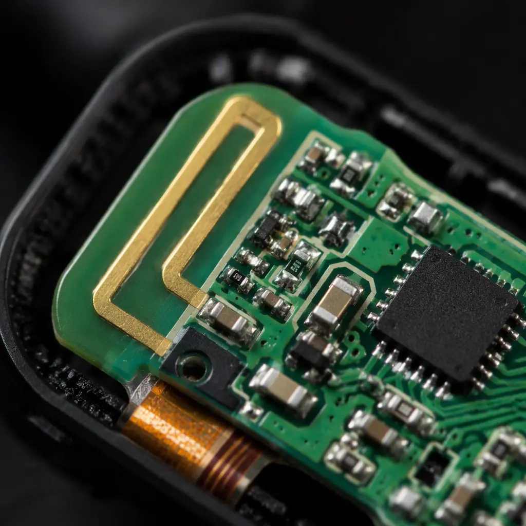
Before any routing starts, the stackup and floor plan must be fixed, because there is no room to move later. The dominant constraint is antenna clearance: the 2.4 GHz antenna needs a keep-out zone of at least 4 mm on the same layer and a clear projection area above and below it, which immediately consumes a corner of the board.
Layer count: 4 or 6, with a dedicated RF reference
Entry-level earbuds use 4 layers (L1 signal, L2 ground, L3 power/signal, L4 ground). Premium buds with ANC and multi-mic arrays move to 6 layers so the codec, RF, and digital domains each get a clean reference plane. The layer under the antenna must be ground-free in the keep-out zone, and the antenna feed must transition to the RF reference plane with a controlled 50 Ω path.
Component count and placement zones
A full-feature bud carries 60–90 components: Bluetooth SoC, audio codec, two MEMS microphones, touch IC, 2–4 MLCCs per rail, a 3.7 V lithium cell connector, and the charge/protect ICs. Partition the board into four zones before placement: RF (antenna + matching + SoC), analog audio (codec + mic inputs), digital (I2C, touch, LED), and power (charger + battery). Keep the analog and digital zones separated by a ground stitch row, see our mixed-signal grounding guide for the technique.
Board thickness and via strategy
Earbud boards are typically 0.4–0.6 mm thick with laser microvias (0.075–0.1 mm) for routing density. Blind vias from L1–L2 are standard; buried vias add cost and are only justified for 6-layer premium designs. Every via in the RF path adds parasitic inductance, keep the antenna feed via count to one, and use the smallest drill the fab supports.
Key Takeaway: Fix the stackup and the antenna keep-out before placement. At 8×12 mm there is no second chance. A re-spin costs 3–4 weeks and the layout is where 80% of TWS field failures are born.
RF Layout: Antenna, Matching, and the 2.4 GHz Link Budget
The single biggest complaint about cheap earbuds is audio dropouts. And the cause is almost always an antenna starved of clearance or a matching network polluted by the digital supply. The link between bud and phone must survive the head blocking the signal path, which means every dB of radiated power and receiver sensitivity counts.
Antenna types: chip vs PCB trace
Chip antennas (e.g., 2.4 GHz ceramic, 1.6 × 0.8 mm) are the default for earbuds because they are repeatable across units and need only a small ground clearance. PCB trace antennas (IFA or meandered) save the component cost but are sensitive to housing plastic thickness and hand position, which shifts the resonance. If you use a trace antenna, specify a tuning stub and require a VSWR ≤ 2:1 across 2400–2483 MHz in the final enclosure, not on the bench. Our PCB antenna design guide covers both options in detail.
The π matching network and its ground return
The SoC RF pin connects through a π network (two shunt caps, one series inductor or 0 Ω) to the antenna feed. The shunt cap grounds must return to the RF reference plane directly under the pad, a long via stub here detunes the network. Keep the entire matching network inside a 2 × 3 mm area with no other traces within 0.5 mm, and never run digital signals under the network.
RF-deaf zones: keep the antenna away from the battery
The lithium cell and its metal can absorb 2.4 GHz energy and shift the antenna resonance by 50–100 MHz. Place the antenna at the end of the bud furthest from the battery, and keep the battery ground connection to the board's main ground, not through the antenna ground plane. This is the most common mistake in first-pass earbud layouts.
ANC and Microphone Routing: The Audio Signal Path
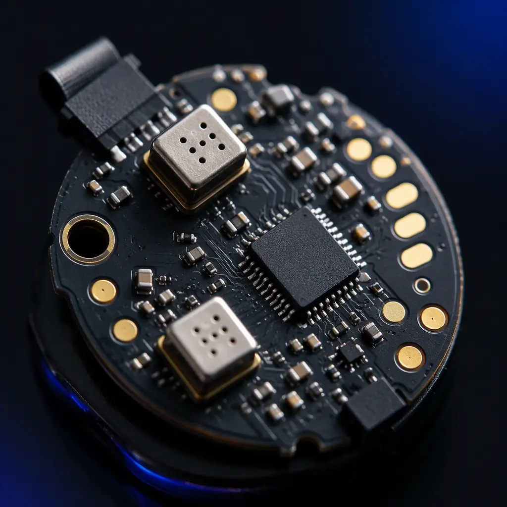
Active noise cancellation lives or dies on the microphone layout. The ANC system compares the reference mic (outside the ear) with the error mic (inside the ear canal) and generates an anti-phase signal; any delay or noise pickup between the two mics destroys the cancellation depth, especially above 1 kHz where the wavelength gets short.
MEMS mic placement and port alignment
Each MEMS microphone has a sound port that must align with an acoustic hole in the enclosure, a 0.1 mm misalignment drops sensitivity by 3–6 dB. On the PCB, route the mic output as a differential pair when the codec supports it (reduces common-mode noise), keep traces under 10 mm, and avoid running them under the battery or the RF section. Add a ground guard trace around each mic input.
Codec placement: as close to the mics as possible
The audio codec should sit within 8 mm of the mic cluster. Every millimeter of trace adds capacitance that rolls off high-frequency response and picks up digital switching noise from the SoC's I2C bus. Route the I2C to the codec as a single trunk with series resistors (22–47 Ω) at the source to damp ringing.
Audio ground: single-point star to the codec AGND
Keep the analog audio ground separate from the digital ground up to the codec's AGND pin, then join them at exactly one point. This prevents the I2C and touch-sense return currents from modulating the mic bias. For the full treatment of analog/digital partitioning, read our mixed-signal design guide.
Charging Case PCB: Power Path and Contact Design
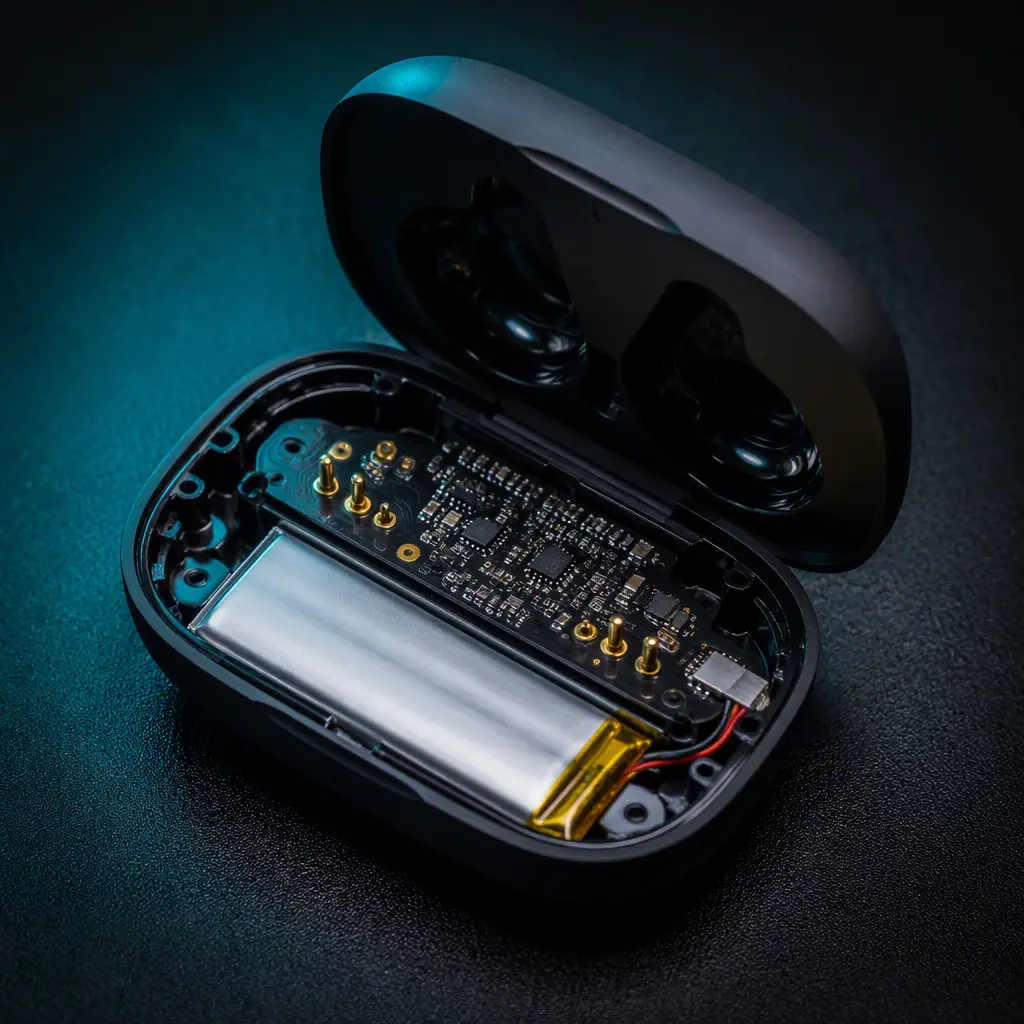
The charging case is electrically simpler than the bud but mechanically brutal: pogo pins or spring contacts must mate thousands of times, and a charging error can damage the case's own battery or the bud's cell. The case board is typically 20 × 30 mm with a 500–1000 mAh cell and a boost converter to deliver 5 V to the buds.
| Design Point | Typical Value | Failure Mode If Ignored |
|---|---|---|
| Case battery | 400–1000 mAh Li-ion | Over-discharge → cell damage |
| Charge current per bud | 100–300 mA at 5 V | Contact resistance heat → plastic deformation |
| Pogo pin current rating | ≥ 0.5 A continuous | Voltage drop → undercharging, false full |
| Boost converter efficiency | ≥ 90% at 200 mA | Case battery drains overnight |
| ESD protection on contacts | ±8 kV contact (IEC 61000-4-2) | Latched-up charger → RMA returns |
Keep the pogo pins off the flex area and stiffen the pads
Spring contacts exert constant force on the solder joints. Use castellated or through-hole mounting for high-cycle contacts, reinforce the pads with copper pour and multiple vias to the inner planes, and never place contacts on a flex tail that flexes during lid open/close. Our edge plating and castellated pads guide shows the via-reinforcement pattern.
Reverse-polarity and short protection on the contacts
The pogo pins are exposed metal. A paperclip or coins in a pocket can short them. Add a PTC fuse and reverse-polarity protection (a low-Vf Schottky or a load-switch with reverse blocking) on the case output, and current-limit the bud charge path at the case side. This is a cheap insurance policy against a recall.
Battery Protection: The Cell You Cannot Afford to Abuse
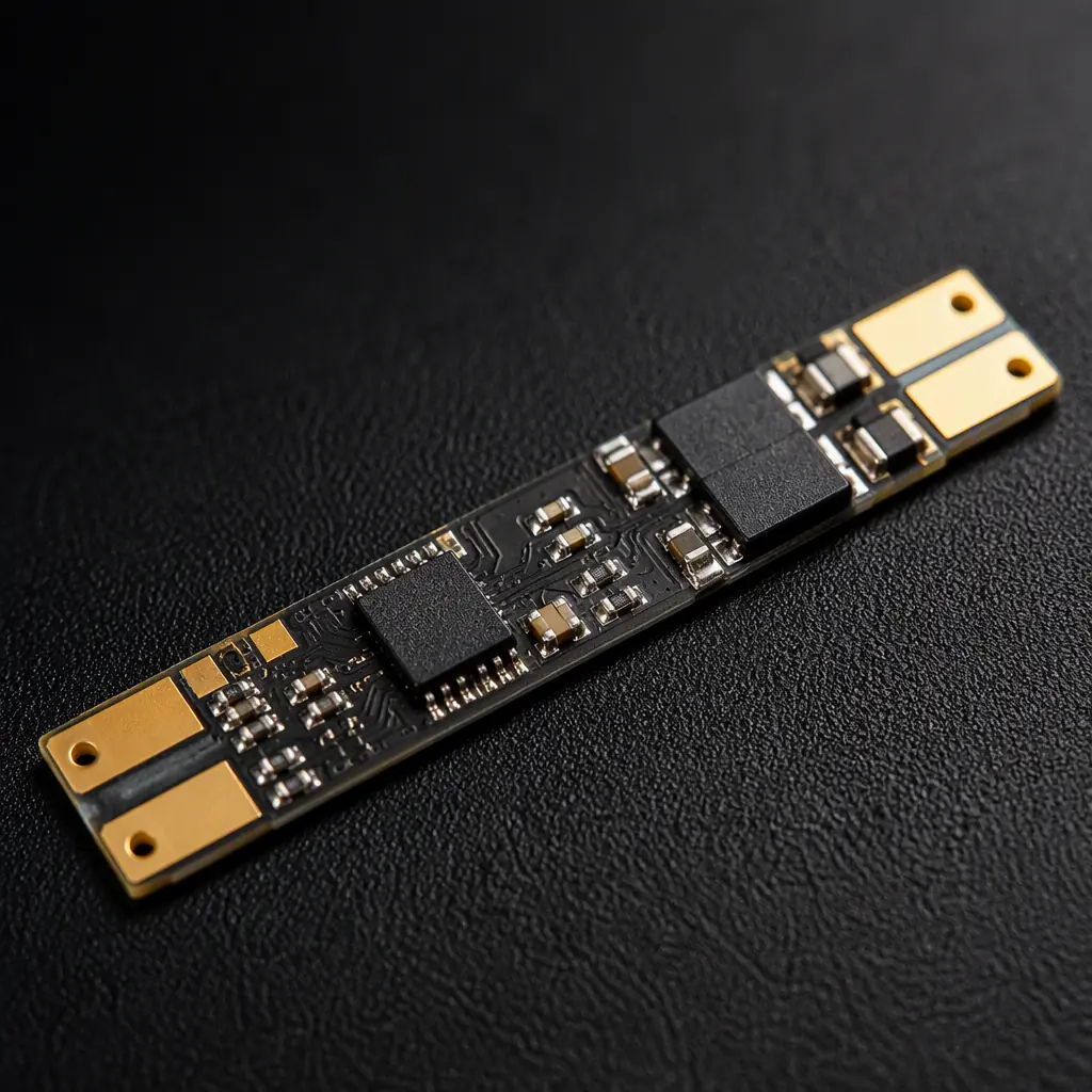
A lithium cell inside an ear canal has zero room for thermal runaway. Every earbud design must include protection at three levels: the cell's own protection IC, the system's charge management, and the firmware's voltage/current limits.
Protection IC + MOSFET pair on every bud board
Place the protection IC (overcharge ≥ 4.25 V, over-discharge ≤ 2.8 V, overcurrent) directly on the bud board next to the battery connector. Route the cell's positive and negative through the protection FETs before they reach the charger or the system rail, no exceptions. For more on cell-level design, see our consumer electronics PCB guide.
Thermal and layout rules for the charging path
The charge FET dissipates heat in a 0.6 mm board with almost no copper mass. Keep the charge current below 0.5 C, fan out the FET's thermal pad with at least 6 vias to the bottom plane, and keep the battery thermistor trace away from the charge current path so the temperature reading is not corrupted by self-heating.
Procurement Tip: When you send a TWS project to a CM, demand the battery datasheet's charge/discharge curves and the protection IC's trip thresholds in writing. A bud that survives 300 charge cycles instead of 500 is a warranty claim you will pay for, at 100k units, that is a six-figure number.
DFM Rules That Protect Yield at 100k+ Units
Small boards magnify every manufacturing tolerance. A 0.05 mm registration error that is invisible on a 200 × 200 mm board can short two traces on an 8 × 12 mm board. The following rules are the difference between 99% yield and 60% yield at volume.
Minimum features for high-yield SMT
For high-volume TWS production, specify: trace/space ≥ 3/3 mil, minimum via pad 0.3 mm, minimum component pitch 0201 (0.4 × 0.2 mm) with 0.2 mm pad width, and stencil aperture ≥ 0.25 mm. Boards below these limits move from standard SMT into specialty territory with lower yield and higher cost. Our fine-pitch SMT guide details 01005/0201 handling.
Panelization and depanelization strategy
Earbud boards ship in panels of 40–100 units to amortize SMT setup. Use V-score for straight edges or tab-routing with mouse bites for irregular outlines, and specify the depanelization method in the fab notes. Laser depaneling is required when components sit within 1 mm of the board edge (common on earbuds). Compare methods in our depaneling comparison guide.
In-circuit test strategy for tiny boards
There is no room for test pads on an 8×12 mm board, so plan for flying-probe testing (no fixture) plus functional RF testing after assembly. Every bud must get a Bluetooth RF test (TX power, frequency error, sensitivity) on a calibrated tester. This is the only way to catch antenna tuning drift across units. See our test method comparison for the trade-offs.
Moisture and handling for small-form boards
Thin boards (< 0.6 mm) absorb moisture fast and warp during reflow. Specify MSL 2 or better for the components, bake panels per MSL guidelines before assembly, and use a reflow profile with controlled ramp rate to avoid board warp. Warpage is the #1 invisible killer of small-board yield.
Choosing a CM for TWS Production
Not every assembly house can run TWS boards profitably. Before you commit a 100k-unit program, verify four capabilities: 0201 and 0.3 mm-pitch BGA placement (most CMs stop at 0402), X-ray inspection for the tiny BGAs and shielded modules, RF functional testing on the line, and laser depaneling. A CM without all four will either reject your boards or silently lower your yield.
At Huaxing PCBA, our 8 SMT lines place 0201 and 0.3 mm-pitch BGA daily, we run X-ray on every BGA joint, and our functional test bench covers Bluetooth RF verification for wearable products. We assemble boards from 6 × 8 mm up to full box-build systems. Send us your Gerber files and BOM for a DFM review. You will get a line-by-line quote with assembly-yield feedback within 24 hours. Contact our engineering team, or continue with our COB vs COG vs SMT assembly guide if you are considering chip-on-board for an ultra-miniaturized design.
