
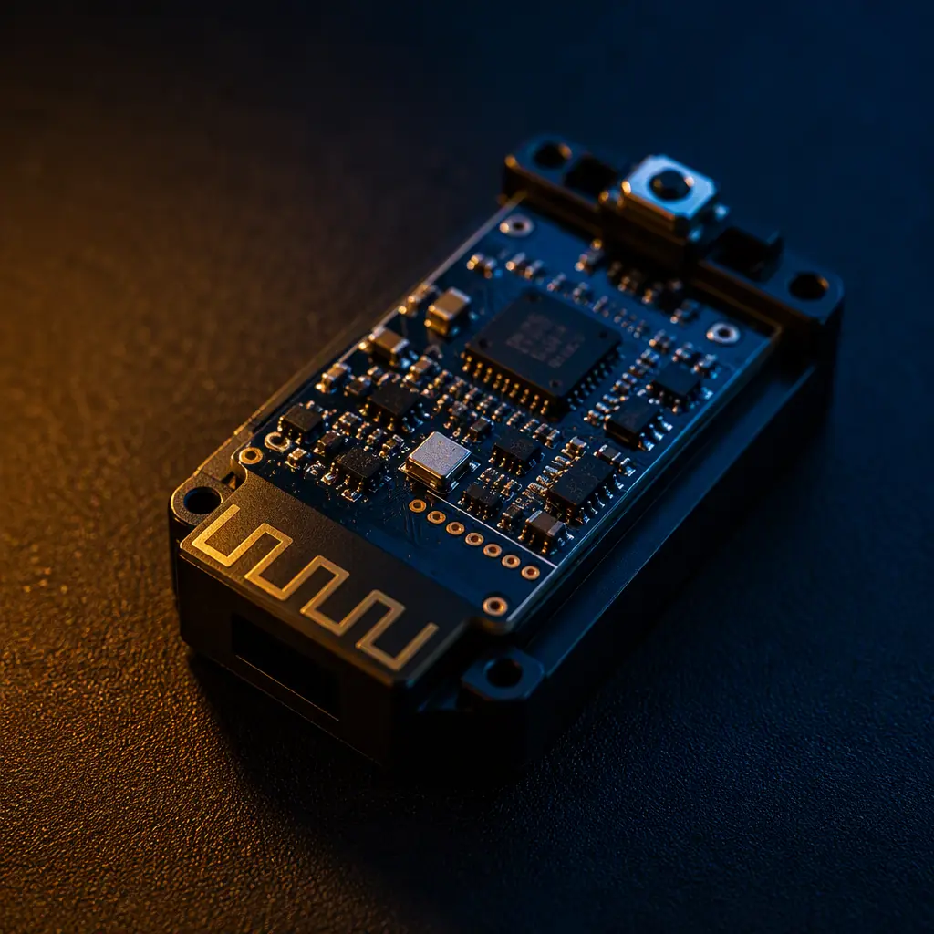
Every wireless product has an antenna problem, and on most of them the antenna is part of the PCB itself: a printed trace antenna, a chip antenna, or the feed to an external element. The antenna is the component with the widest performance spread relative to its cost — the same radio chip can deliver 20 dB of additional link budget with a well-designed antenna versus a badly placed one, which is the difference between a product that works across a warehouse and one that drops connection across a room. And unlike every other component, its performance depends on things you cannot buy: the ground plane, the clearance, the enclosure, and the tuning.
Huaxing PCBA manufactures wireless boards for BLE, Wi-Fi, sub-GHz, and cellular products — controlled-impedance RF stackups, mixed laminates, antenna keep-out verification in DFM, and RF functional testing on the assembly line. This guide covers the antenna types, the design method for a 2.4 GHz trace antenna, matching network tuning, the layout rules that preserve range, and how to test the result.
Antenna Types Compared
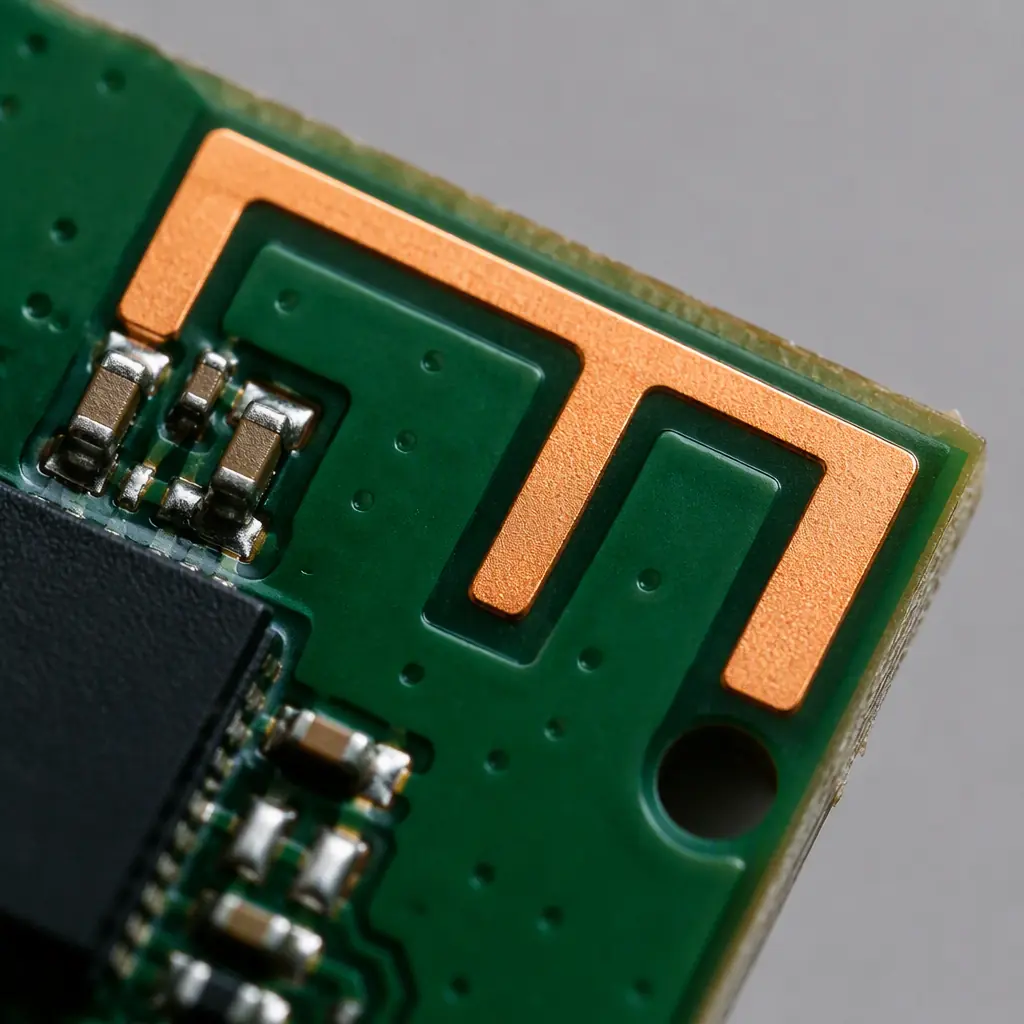
The choice between a trace antenna, a chip antenna, and an external antenna is a size/cost/performance trade. Most products land on a trace or chip antenna; external antennas appear when range is a hard requirement.
| Antenna Type | Typical Size (2.4 GHz) | Efficiency | Tuning Effort | Best For |
|---|---|---|---|---|
| Inverted-F (IFA) trace | ~15.5 × 6 mm | 60-80% | Medium — trim + match | BLE, Wi-Fi, Zigbee products |
| Meandered (MIFA) trace | ~10 × 5 mm | 50-70% | Medium-high | Compact wearables, sensors |
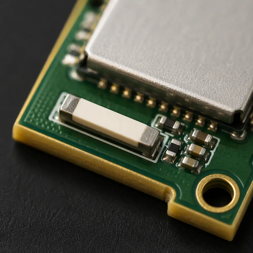
| Chip antenna | 1.6 × 0.8 to 7 × 2 mm | 50-75% | Low-medium — datasheet layout | Very small boards, modules |
| External (whip, dipole, PCB panel) | 25-100 mm | 70-90%+ | Low — plug and play | Gateways, routers, industrial links |
A trace antenna costs nothing but board area and needs the most engineering attention. A chip antenna costs $0.10-0.50 and shrinks the footprint but imposes strict datasheet layout rules. An external antenna costs the most and takes space but delivers the best, most predictable performance. Our BLE PCB design guide and Wi-Fi design guide show how each choice plays out in a specific radio context.
How a PCB Antenna Works: Resonance, Ground Plane, and Bandwidth
Understanding the physics behind the antenna saves you from the two classic mistakes: copying a reference layout into the wrong board shape, and "tuning" without understanding what you are tuning.
The Antenna Is Half the Circuit — the Ground Plane Is the Other Half
An inverted-F antenna is a quarter-wave structure: the radiating element plus the board's ground plane together form the antenna. The ground plane is not a passive backdrop — its size, shape, and the copper beneath the antenna directly set the resonant frequency and efficiency. This is why the same antenna design behaves differently on a 20 × 30 mm sensor board and a 50 × 80 mm product board, and why antenna layout must be locked before the board outline is final.
Resonance Is Set by Electrical Length, Not Physical Size Alone
At 2.4 GHz a quarter wavelength in free space is about 31 mm. A trace antenna achieves resonance in a smaller footprint using the dielectric of the board (which shortens the wavelength) and the meandering of the trace. The exact resonant frequency depends on trace geometry, dielectric constant, ground plane, and even the solder mask. That is why the final frequency is trimmed on the bench, not computed once.
Bandwidth Is the Price You Pay for Small Size
Small antennas are narrowband. A compact trace antenna may cover only 100-200 MHz of bandwidth — enough for one band (BLE's 2.4-2.483 GHz, or Wi-Fi's lower channels) but not the full 2.4 GHz ISM range with margin in a plastic-enclosure shift. If your product must work across the whole 2.4 GHz band plus handle enclosure detuning, budget for a wider antenna design or accept a tuned compromise.
Key Takeaway: The ground plane is half the antenna, resonance is set by electrical length, and small antennas are narrowband. Design the board outline and antenna together — never drop a reference antenna into a board shape it was not designed for.
Designing a 2.4 GHz Trace Antenna (IFA)
The inverted-F antenna is the workhorse of 2.4 GHz product design. It is compact, cheap, and well documented — TI's AN043 reference and Nordic's antenna notes are the starting points most engineers use. The dimensions below are the classic starting values; your tuning will adjust them.
Start From a Proven Reference Geometry
A 2.4 GHz IFA typically occupies about 15.5 × 6 mm: a radiating arm of roughly 12-15 mm, a shorting stub of 1-2 mm connecting the antenna to ground at the feed end, and a feed point placed along the arm. The antenna sits at the board edge or corner with nothing beneath it but the board's ground pour — the clearance zone extends below the antenna on all layers. Use the reference design's dimensions verbatim as your starting point.
Size the Ground Plane Correctly
Reference designs assume a ground plane of at least 20 × 40 mm under and beside the antenna. Smaller ground planes shift the resonance up and hurt efficiency; larger ones are fine. If your board is smaller than the reference assumption, expect to tune more aggressively — or move to a chip antenna with a layout specified for small grounds.
Feed It With a 50 Ω Line and a Tuning Stub
The feed from the radio's matching network to the antenna is a 50 Ω trace (typically 0.4-0.6 mm wide on a 0.8-1.6 mm FR-4 stackup, depending on the layer). Add a small tuning stub or a provision for a series inductor at the feed so the bench can adjust impedance without cutting copper. Our impedance control guide covers how to specify the feed's impedance on the fab drawing.
Meander Only When You Must
Meandering the trace (MIFA) shrinks the antenna but narrows the bandwidth and makes tuning touchier. For a product with a fixed, known frequency band it is a fair trade; for a multi-channel radio it is not. If the board has room for a straight IFA, use it.
Chip Antennas: When to Use Them and the Datasheet's Hidden Rules
Chip antennas solve the "no room for a trace" problem and are heavily used in wearables, hearables, and compact modules. They are not simpler — they just move the complexity into a very strict layout recipe.
The Datasheet Layout Is the Antenna
Chip antenna datasheets specify a ground clearance area (often a notch or a region with no ground pour on the layer below), a recommended placement (usually a board corner or edge), and a matching network. Copy the recommended layout exactly — including the clearance geometry. Vendors provide antenna evaluation boards and layout guides for a reason: the antenna only works as specified with that exact surrounding copper.
Keep the Matching Network Close and Symmetric
The chip antenna's matching components (typically a π network of two shunt caps and a series inductor) sit within a few millimeters of the antenna feed. Keep the traces between them short and symmetric, ground the component pads directly to the antenna's ground area, and do not route other signals through the clearance zone on any layer.
Watch Out for Battery and Enclosure Proximity
A lithium battery under the antenna clearance absorbs radiation and detunes the antenna — a classic cause of "works on the bench, fails in the product." Keep the battery, metal brackets, and large ground pours out of the antenna's near field (a few millimeters for 2.4 GHz, more for sub-GHz). Test the final assembled product, not the bare board. Our RFID/NFC antenna guide shows the same proximity logic applied to NFC coils.
The Matching Network: 50 Ω, the π Network, and Tuning on the Bench
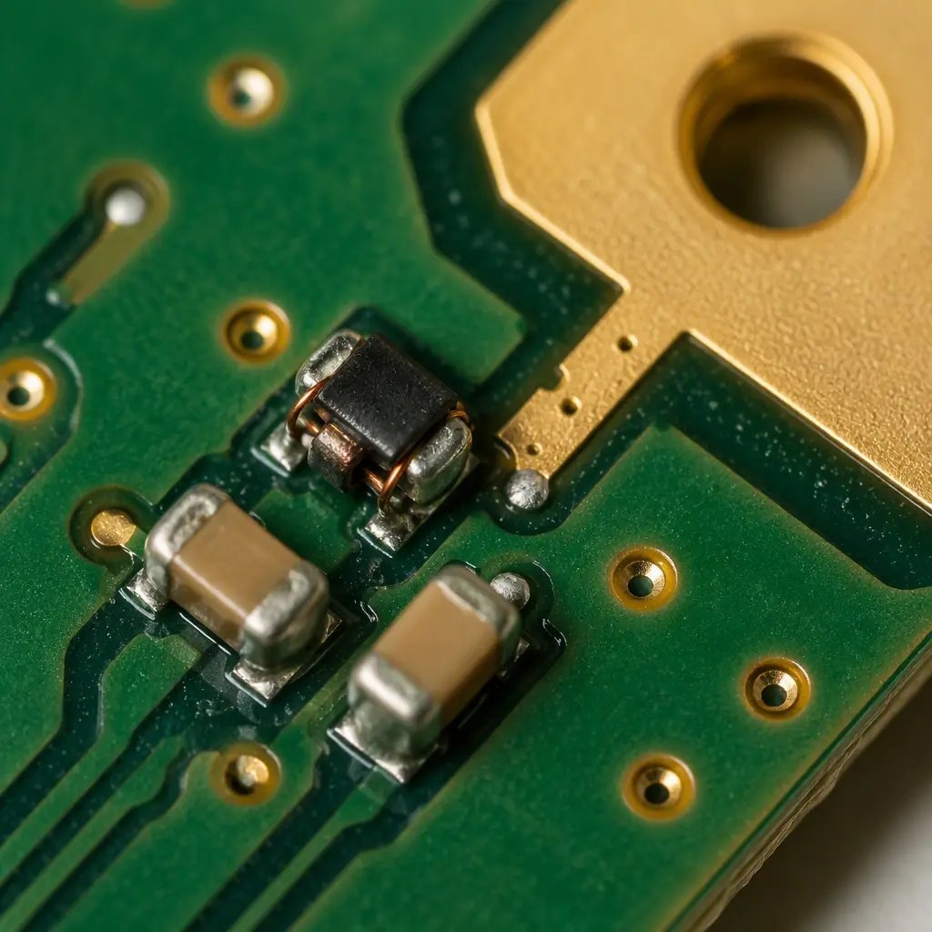
The antenna's impedance at its feed point is rarely exactly 50 Ω — the matching network transforms it so the radio sees a clean 50 Ω load, maximizing power transfer and minimizing reflections.
Design for a π Network With Tuning Positions
Reserve a π network at the antenna feed: one series element and two shunt positions (typically a 1-10 nH inductor in series with 0.5-2 pF capacitors to ground, values depending on the antenna and band). On the first prototype, populate the network with placeholder values from the reference design, measure, then adjust. Populate the pads with 0402 or 0603 parts so values can be swapped during tuning.
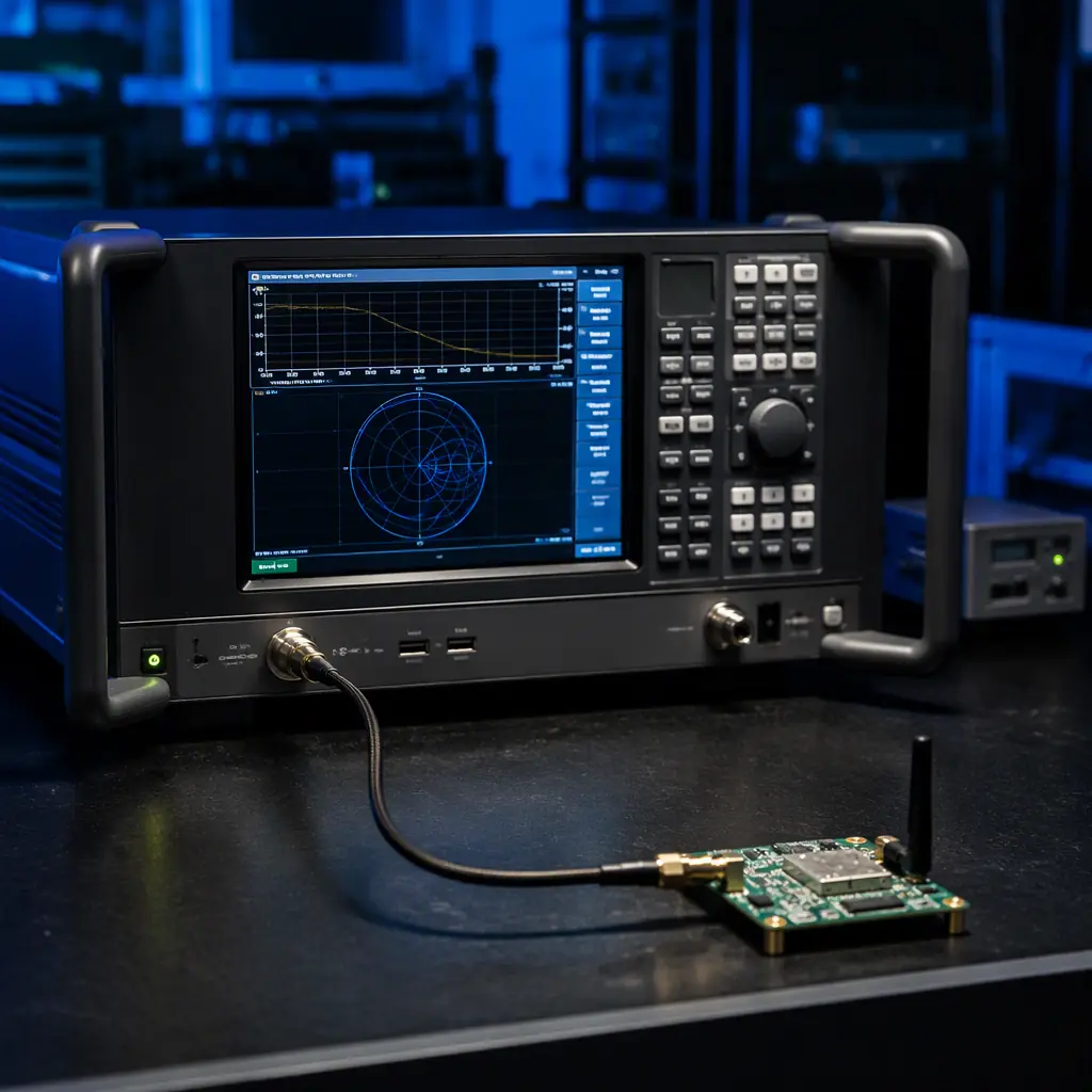
Tune With a Vector Network Analyzer, Not by Range Testing
The correct tuning instrument is a VNA measuring return loss (S11) at the antenna feed. The target is return loss better than -10 dB (VSWR under 2:1) across your operating band, with -15 dB or better at the center frequency. Range testing alone cannot separate antenna problems from radio, firmware, or environment problems — it only tells you the total is bad. A 30-minute VNA session at the start of a project saves weeks of field debugging later.
Retune in the Final Enclosure
The enclosure shifts the antenna — plastic with high dielectric constant lowers the resonant frequency; metal shields and batteries absorb energy. Tune the antenna with the product assembled in its final enclosure, with the battery installed, and with the same orientation the product will be used in. A design tuned on the open bench and then placed in an enclosure is a design tuned to the wrong environment.
Layout Rules That Kill Range
These are the mistakes seen most often in DFM reviews of wireless boards — each one costs measurable dB of real-world performance.
Copper in the Keep-Out Zone
Ground pour, traces, or component pads in the antenna clearance — on any layer — detune the antenna and short the radiation. The clearance must be enforced on all layers, including inner planes. This is checked in DFM; boards arrive with antennas that cannot work because an inner-layer ground plane extends under the antenna.
Traces Running Under or Beside the Antenna
Digital lines, power traces, or the crystal's routing under the antenna couple noise into the radiator and shift its resonance. Keep all routing out of the antenna zone, and route the radio's crystal and supply lines away from the antenna side of the board.
Solder Mask and Silkscreen Over the Antenna
Covering the trace antenna with solder mask changes its resonant frequency by a measurable amount. Specify mask removal over the antenna element, and keep silkscreen and reference designators out of the zone. Our solder mask guide covers how to specify mask openings.
Uncontrolled Feed Impedance
The 50 Ω feed between the radio and the antenna must actually be 50 Ω. On a stackup where the fab did not control impedance, the feed's mismatch adds directly to the system's return loss. Specify impedance control on the RF feed and verify with coupons. See our RF PCB manufacturing guide for the fabrication requirements.
Antenna Testing: Return Loss, VSWR, and Radiated Performance
Testing has two levels: conducted (at the feed point, with a VNA) and radiated (over the air, in a chamber or anechoic environment). Both belong in the product's test plan.
Conducted: Return Loss and VSWR on Every Design Iteration
Measure S11 at the antenna feed over the operating band on each prototype iteration. Record the return loss curve and the resonant frequency; both should be stable across a few boards (part tolerance and laminate variation cause small shifts). If the resonance jumps between boards of the same design, check the fabrication for stackup or material drift.
Radiated: TRP and TIS for the Full Picture
Total Radiated Power (TRP) and Total Isotropic Sensitivity (TIS) measure what the antenna actually radiates and receives over the air — the numbers that matter for range. A chamber or anechoic measurement gives you these, and it is the only reliable way to compare antenna designs or enclosures. For certification, radiated testing is mandatory anyway.
Production: RF Functional Test on the Line
On the assembly line, a simple RF functional test — transmit power and frequency at the antenna connector, or a radiated sniff test in a shielded fixture — catches assembly defects (missing components, solder bridges in the matching network, damaged antennas) before units ship. For high-volume wireless products this test is standard. Our testing methods guide places RF tests in the full test strategy.
DFM Checklist: What to Send the Fab
The fabrication drawing for a board with an on-PCB antenna needs a few specific notes beyond the standard set:
Impedance Control on the RF Feed
Specify the 50 Ω feed's impedance target and tolerance (±10% typical, tighter if your design requires it), with coupons on every panel and reported data. The coupon stackup must match the real board — same dielectric thickness and trace geometry. Our stackup design guide shows how to define the RF stackup.
Mask Removal Over the Antenna
Note the mask opening over the trace antenna element so the fab does not cover it. If the design uses a specific laminate or copper weight for the RF layer, state it — mixed-stackup wireless boards are routine, but only when the drawing says so.
DFM Review of the Keep-Out
Ask the manufacturer to verify the antenna keep-out on all layers as part of DFM. A good fab will flag copper in the antenna zone before tooling, saving you a respin. This review is included free with every Huaxing quote — it has caught real antenna problems on wireless projects of every size.
Summary: The Antenna Design Checklist
A wireless product with real range has an antenna that was designed, not assumed: the right antenna type for the board size and band, a ground plane sized to the reference design, a clean keep-out on every layer, a 50 Ω feed with controlled impedance, a π network tuned with a VNA in the final enclosure, and a production test that catches assembly defects. Every step is cheap compared with the cost of a product that drops connection in the field.
At Huaxing PCBA we manufacture wireless boards with controlled-impedance RF stackups to ±5%, mixed FR-4 and high-frequency laminates, mask openings and keep-out verification in DFM, and RF functional testing on 8 SMT lines. Our DFM review checks the antenna clearance on all layers, the feed impedance stackup, and the assembly requirements before tooling. Read our GNSS antenna guide for the positioning side of antenna design, or send your files for a free DFM review and quote.
