
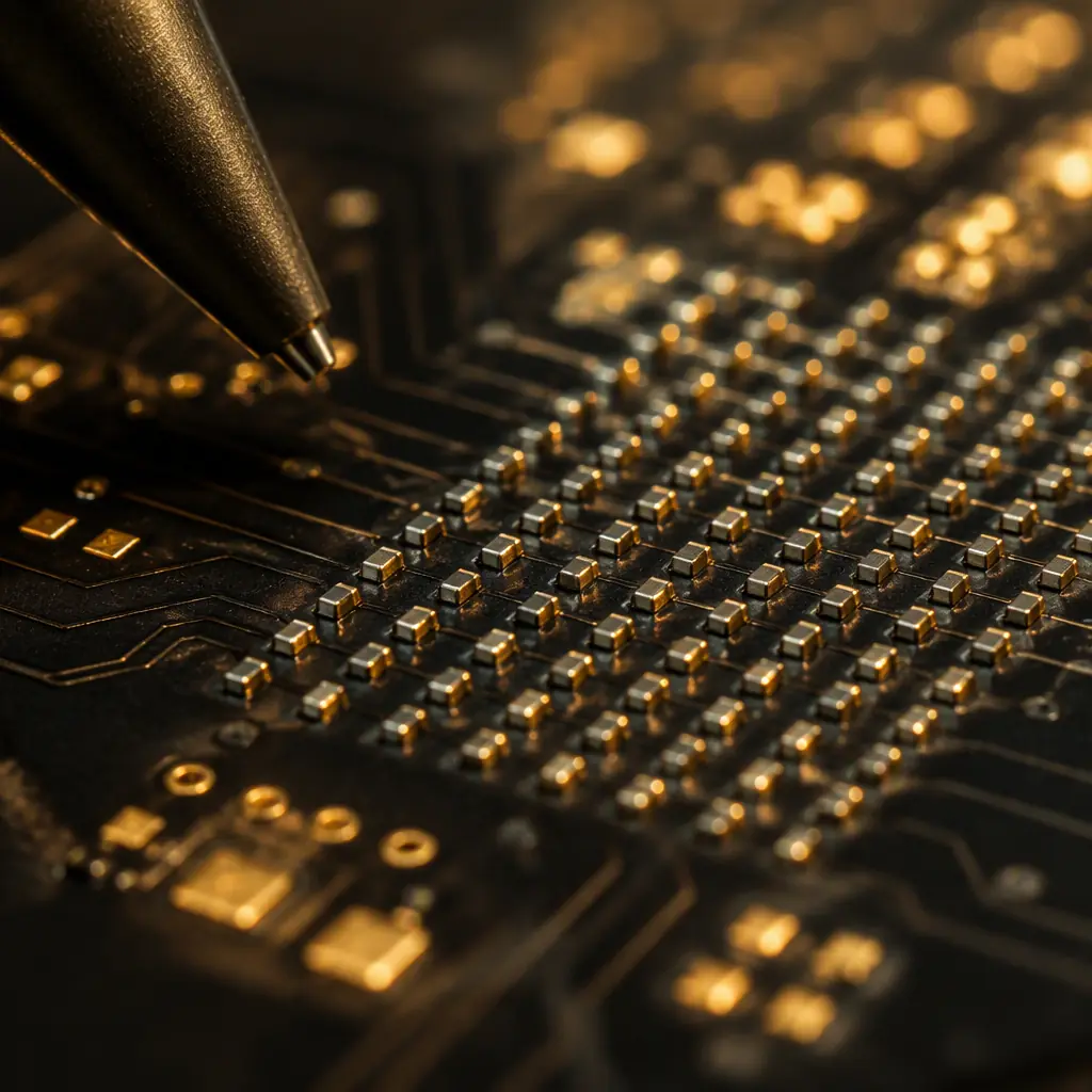
A 01005 resistor is 0.4 mm × 0.2 mm — about the size of a grain of salt. A 0.4 mm-pitch QFP has leads just 0.16 mm wide with 0.24 mm gaps. Both are routine in wearables, hearing aids, modules, and any product where every square millimeter of PCB costs money. The difference between a factory that assembles these parts at 99.5% first-pass yield and one that scrapes by at 96% is not luck — it is a specific, measurable process stack: placement machine capability, stencil geometry, solder paste particle size, reflow profile control, and inspection resolution. This guide walks through each layer and what to demand from your assembler when your BOM contains fine-pitch parts.
Huaxing PCBA runs fine-pitch production on 8 SMT lines with 3D SPI and 3D AOI on every line, qualified for 01005 and 0.3 mm-pitch CSP assembly. The numbers below are the actual process parameters our engineers quote against — use them as the yardstick when you evaluate an assembly partner.
What "Fine Pitch" Actually Means on an Assembly Line
"Fine pitch" covers two distinct families of parts, and each stresses a different part of the process:
| Component | Size / Pitch | Critical Process Stress |
|---|---|---|
| 0201 chip (0603 metric) | 0.6 × 0.3 mm | Stencil printing, tombstoning |
| 01005 chip (0402 metric) | 0.4 × 0.2 mm | Placement accuracy, paste volume control |
| 008004 chip (0201 metric) | 0.25 × 0.125 mm | Placement accuracy, AOI resolution, handling |
| QFP / SOP | 0.3 - 0.5 mm lead pitch | Print definition, bridging control |
| CSP / BGA | 0.3 - 0.5 mm ball pitch | Aperture design, X-ray verification |
Once lead pitch drops to 0.5 mm or below — or passives drop to 0201 and smaller — the assembly process shifts from "standard" to "fine-pitch mode": thinner stencils, finer paste, tighter placement tolerances, and higher-resolution inspection. Each of the next five sections covers one layer of that stack.
Placement: The ±40 μm Accuracy Reality
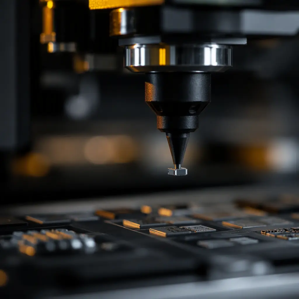
The placement machine is the first gate. For 01005 components, industry-standard capability requires placement accuracy of ±40 μm at 3σ (Cpk ≥ 1.33, with most leading lines quoting Cpk ≥ 1.67). That is roughly one-tenth of the component's own width. A machine rated ±80 μm can assemble 0402 parts all day but will scatter 01005 parts across the pad — and the defect appears downstream as tombstoning, reflow misalignment, or opens that AOI catches only after reflow, when rework is expensive.
Verify the Machine Class, Not the Marketing Sheet
Ask the assembler for the placement Cpk measured on your board type with glass slide or fiducial-based verification, not the machine vendor's datasheet number. A useful audit question: "What is your measured placement accuracy for 01005, and when was it last verified?" The honest answer includes a date and a procedure (typically IPC-9850 or the machine maker's calibration glass). Our supplier audit guide includes this as a line item in the process-capability section.
Fiducials and Panel Stiffness Are Part of Accuracy
The machine's accuracy is only as good as the board's positional reference. Every panel needs global fiducials plus local fiducials within 10 mm of fine-pitch sites. Panel stiffness matters equally: a 0.8 mm board that bows more than 0.5% during placement pushes parts off their pads before reflow even starts. See our panelization guide for the rail/fiducial geometry rules.
Nozzle and Force Control for Tiny Bodies
01005 parts need dedicated mini-nozzles (typically 0.3-0.5 mm ID) and placement force of 0.5 - 2.0 N with closed-loop force control. Too little force — the part sticks to the nozzle; too much — paste squeeze-out and pad damage. Air-pressure and vision centering must be replaced with laser or 3D centering for these sizes.
Stencil: The 0.08 mm Laser-Cut Reality
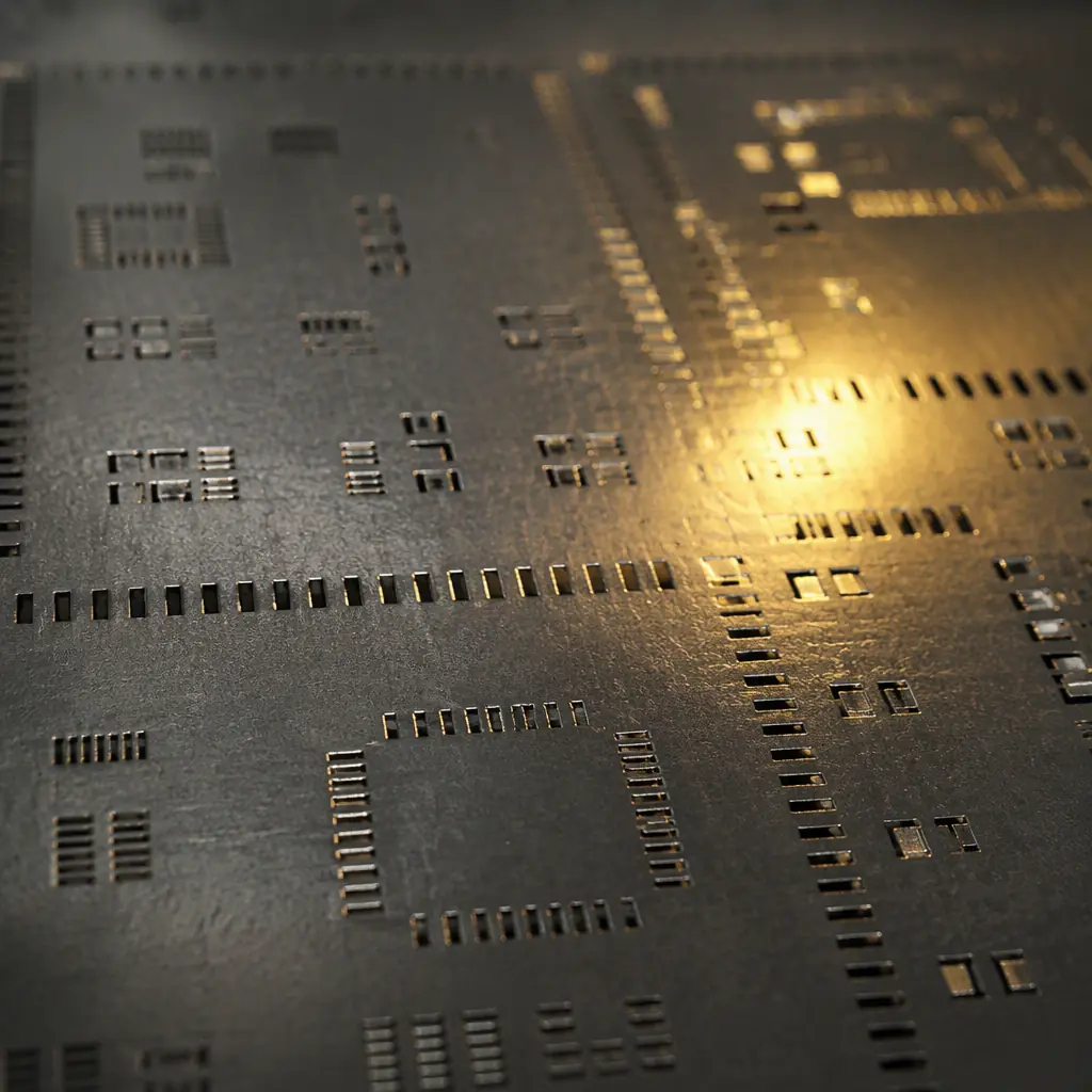
The stencil is where fine-pitch yield is won or lost, because print defects are the single largest cause of reflow defects. For 01005 and 0.3 mm-pitch work, the baseline is a 0.08 mm (3 mil) laser-cut stainless stencil — versus 0.12-0.15 mm for standard 0402+ assemblies — with aperture walls cleaned by electropolishing or nano-coating to maximize paste release.
Aperture Area Ratio: Keep It Above 0.66
Per IPC-7525, the aperture area ratio (opening area ÷ wall area) must stay above 0.66 for reliable paste release. For a 01005 pad of roughly 0.22 × 0.22 mm on a 0.08 mm stencil, that works out to an aperture around 0.17-0.19 mm — near the practical limit for laser cutting. Below 0.66, paste stays in the aperture and you get skipped deposits, which reflow into opens. Our stencil design guide includes the full calculation table.
Electroformed Stencils for Sub-0.3 mm Apertures
When apertures drop below 0.2 mm, laser-cut walls develop taper and roughness that hurt release. Electroformed (EF) stencils deliver near-vertical, mirror-smooth walls and are the standard choice for 0.3 mm-pitch CSP and 008004 work. They cost more and wear differently — acceptable when your BOM is genuinely fine-pitch.
Print Process: Underside Wiping and Vision Alignment
Fine-pitch printing requires automatic underside wiping every 5-10 prints (versus 20-30 for standard work), a print speed of 20-50 mm/s, and a snap-off of 0-0.5 mm. Board-to-stencil alignment must use vision with the fine-pitch fiducials — pin alignment alone will not hold ±25 μm print registration.
Solder Paste: Type 4/5 Powder and a Controlled Environment
Paste particle size must fit through the aperture. IPC J-STD-005 powder types: Type 4 = 20-38 μm, Type 5 = 15-25 μm, Type 6 = 5-15 μm. Rule of thumb: aperture width should be at least 5× the largest particle. A 0.18 mm aperture needs Type 4 at minimum and Type 5 for reliable release. Type 5's trade-off is faster oxidation (more surface area) — which is why fine-pitch paste is used within an 8-hour stencil life and refrigerated at 2-10°C with a 72-hour opened-shelf limit.
Key Takeaway: Fine-pitch printing is a humidity-controlled operation. The paste responds to ambient conditions — target 20-26°C and 40-60% RH in the print room. Below 40% RH, static and paste drying; above 60%, paste absorbs moisture and spatters in reflow, causing solder balls around 01005 joints — the defect class most often blamed on the paste but actually caused by the environment. Our solder paste selection guide covers alloy and flux choices for each powder type.
Reflow: Winning the Tombstone and Solder-Balling Battle
Two defect modes dominate fine-pitch reflow, and both are controlled by the profile and the layout:
Tombstoning: The Wetting-Balance Problem
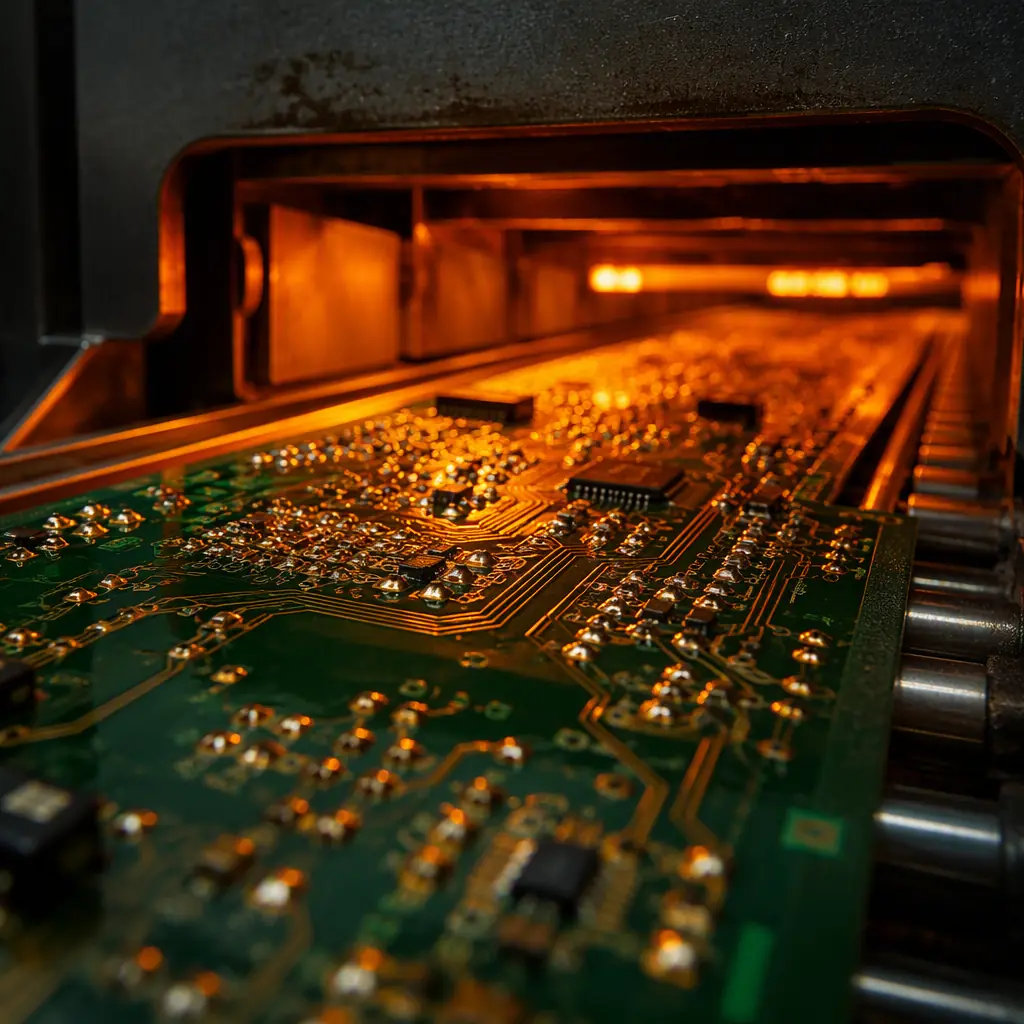
Tombstoning happens when one end of a chip component wets and pulls before the other. For 0201/01005 parts, the trigger is usually asymmetric pad sizes, a thermal gradient across the component, or paste volume mismatch between the two pads. The profile countermeasure is a controlled ramp: ≤ 2°C/s preheat ramp and a soak at 150-200°C for 60-120 s to equalize component temperature before liquidus. Paste-volume asymmetry on fine-pitch pads is detected at SPI, not after reflow — which is why 3D SPI on every print is non-negotiable for fine-pitch boards.
Solder Balls: Environment + Profile
Solder balls around fine-pitch joints come from paste spatter (moisture pickup or too-fast ramp into liquidus) or from paste printed outside the pad. For SAC305, keep time above liquidus at 60-90 s, peak at 235-245°C, and consider nitrogen reflow for sub-0.4 mm pitch — nitrogen (O₂ < 1000 ppm) reduces oxidation-driven solder balling and improves wetting on tight geometries. Our reflow profile optimization guide gives the full parameter table for SAC305 and lead-free alloys.
Pad Design Is a Process Input, Not Just a Layout Choice
Many fine-pitch yield problems are designed in: asymmetric thermal relief, vias-in-pad without fill that steal paste, and solder-mask-defined pads that shrink the effective paste area. The fix belongs in DFM review before the stencil is cut — our DFM tips guide and design-for-test guide list the fine-pitch pad rules (NSMD pads, filled vias, balanced thermal relief) that prevent the tombstone and void defect families at the source.
Inspection: Seeing What You Built
If you cannot inspect a defect class, that defect class is shipping. Fine-pitch demands a three-layer inspection stack:
3D SPI After Every Print
SPI measures paste height, area, and volume on every pad — catching the skipped deposits and volume asymmetry that become opens and tombstoning after reflow. For 01005 pads, SPI must resolve ±10 μm height differences; a 2D SPI cannot see the volume defect on a 0.22 mm pad.
3D AOI at ≥ 10 μm Resolution
Post-reflow AOI needs a camera resolution of 10 μm/pixel or better for 01005 and 0.3 mm-pitch parts (5 μm for 008004), with 3D height measurement for solder fillet volume and lead-lift detection on QFPs. 2D AOI at 15-20 μm will miss the lifted lead and the marginal fillet that fails in vibration testing. Our AOI/X-Ray/SPI comparison covers the resolution and coverage trade-offs.
X-Ray for CSP/BGA and QFN Hidden Joints
For area-array parts on the same board — even if the fine-pitch content is mostly QFPs — X-ray sampling verifies the hidden joints, including void limits per IPC-7095 (≤ 25% ball area Class 2, ≤ 15% Class 3). Our BGA assembly guide covers the X-ray acceptance workflow, and the flip-chip substrate guide explains the fine-pitch side of advanced packaging.
The Fine-Pitch Qualification Checklist
When you move a design with 01005/0201 or sub-0.5 mm-pitch ICs to a new assembler, run this before committing production volume:
Machine Capability Evidence
Placement Cpk ≥ 1.33 (prefer 1.67) verified for your smallest component size, with a dated procedure.
Stencil Design Review
Aperture area ratio ≥ 0.66 on every fine-pitch pad; stencil thickness and finish (laser + nano-coat vs electroformed) matched to your smallest aperture.
Paste Qualification
Powder type (Type 4 minimum, Type 5 for < 0.3 mm apertures), storage and stencil-life controls documented.
Environment Logging
Print room temperature/humidity monitored and logged — ask to see the last 30 days of data.
Inspection Coverage
3D SPI + 3D AOI at the resolutions above, X-ray available for area-array parts, and first-article inspection against your acceptance criteria. Our FAI guide lists the complete first-article package.
First-Article Build and Report
Run a pilot panel through the full line, then review SPI volume data, AOI images, X-ray results, and electrical test before production sign-off. See our testing methods guide for the electrical test options at fine pitch (flying probe versus fixture-based ICT).
How Huaxing PCBA Runs Fine-Pitch Production
Fine-pitch is our default, not our specialty line: all 8 SMT lines are equipped for 01005 and 0.3 mm-pitch work, with 3D SPI and 3D AOI on every line, X-ray for area-array parts, and print-room climate control at 20-26°C / 40-60% RH. We maintain measured placement Cpk records per line, cut stencils in-house with nano-coating, and qualify paste per BOM. Send us your design files — we will run the fine-pitch DFM review (pad geometry, aperture ratio, panel stiffness) and return a quote with the process parameters for your smallest part, before you commit a single panel.
Upload your fine-pitch design for DFM review and a 24-hour quote, or read our quote comparison guide to see how to evaluate assembly proposals for fine-pitch work.
