
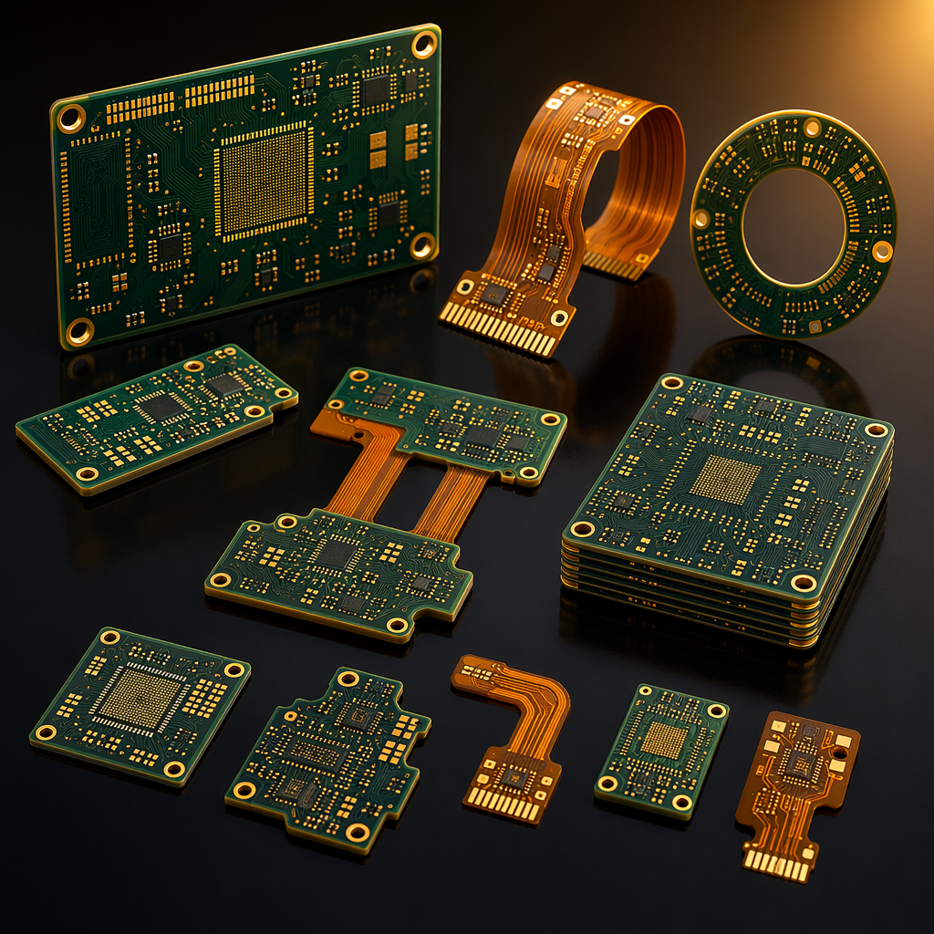

HDI, High-Density Interconnect, is not a single technology. It is a family of PCB fabrication methods that use microvias (laser-drilled holes under 0.15mm), buried vias, and sequential lamination to pack more interconnections into less board area. At Huaxing PCBA, we manufacture HDI boards from simple 1+N+1 structures up to any-layer (every layer pair connected by microvias) on boards with 32 layers. But the engineering question most designers face is simpler: "Is this board dense enough to justify HDI?"
Decision threshold: If your board design has more than 0.4 BGA components per square centimeter or requires trace widths below 4 mils to fit routing, HDI is almost certainly justified. Below that threshold, a standard through-hole design on the same layer count almost always costs less.
Microvias vs Through-Holes: The Physics of Density
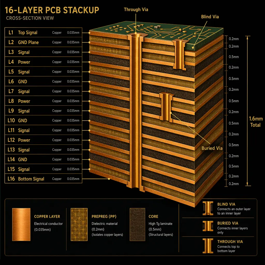
A standard through-hole via goes all the way through the board: every layer, top to bottom. On a 12-layer board, that via occupies real estate on all 12 layers, even if it only connects layers 1 and 2. On a dense BGA breakout, those wasted pads on layers 3–12 block routing channels that you cannot afford to lose.
A microvia solves this. Laser-drilled from the outer layer to the layer directly beneath it, a microvia occupies space on exactly two layers, the ones it connects. Layers below remain untouched, free for routing. The result: on a board with a 0.8mm pitch BGA, moving from through-hole vias to microvias typically frees 30–40% of routing channels on internal layers.
0.15mm
Minimum mechanical drill diameter for standard through-hole vias. Below this, you need laser-drilled microvias: typically 0.075mm to 0.1mm. The transition from mechanical to laser drilling is the engineering boundary between standard and HDI fabrication.
HDI Structures: 1+N+1 to Any-Layer
HDI complexity is defined by the number of sequential lamination cycles and microvia layers. The notation is standard across the industry:
1+N+1 (One Build-Up Layer)
One microvia layer on top, one on bottom, with a standard core of N layers in between. The microvias connect the outer layers to the first inner layer beneath them. This is the most common HDI structure. Used in smartphones, tablets, and automotive ADAS modules where board space is constrained but not extreme. At Huaxing, a 1+6+1 board (8 layers total) adds roughly 15–20% to the fabrication cost compared to a standard 8-layer through-hole board.
2+N+2 (Two Build-Up Layers)
Two stacked microvia layers on each side, enabling blind connections from the surface to the second internal layer. Common in high-performance computing modules, FPGA carrier boards, and aerospace where multiple BGA packages with different pin densities share the same board. The sequential lamination adds a second press cycle, which increases lead time by 3–5 business days and fabrication cost by 30–40% over a 1+N+1 structure.
Any-Layer HDI
Every layer pair is connected by microvias. There are no through-hole vias, no mechanical drills: every interconnection is laser-formed. On a 10-layer any-layer board, that means 9 microvia layers. This is the highest-density HDI structure, used in premium smartphones, military radar modules, and medical implantables. The process requires a separate lamination cycle per layer pair, which pushes lead time to 15–20 business days and fabrication cost to 2–3× that of an equivalent-layer-count standard board.
+15–20%
Typical cost adder for 1+N+1 HDI over standard through-hole on the same layer count. For 2+N+2, the adder is 30–40%. For any-layer, it is 100–200%. The decision to use HDI should be driven by whether the board area savings or performance gains justify that premium, not by default.
When HDI Is Worth the Cost
HDI is not always the right choice, even when a board has high component density. The economics depend on what the denser routing actually achieves:
Board Area Reduction That Eliminates a Layer Pair
The most common justification: a 10-layer standard board can be reduced to an 8-layer 1+N+1 HDI board because the microvias free enough routing space to eliminate two internal signal layers. Removing two layers reduces raw material cost, lamination cycles, and drilling time, partially offsetting the HDI premium. The net cost difference is often under 10%, and the thinner board improves thermal performance and reduces weight.
BGA Escape Where Standard Vias Fail
When a BGA package drops below 0.8mm pitch, standard through-hole vias between pads become geometrically impossible, the annular ring requirements consume the available space between pads. At 0.5mm pitch and below, microvias are not a choice; they are the only routing option. The cost question is moot because the alternative is an unmanufacturable board.
Signal Integrity at Speed
Through-hole vias create stubs, unused portions of the via barrel that extend past the signal layer. At frequencies above 5 GHz, these stubs become quarter-wave resonators that degrade signal integrity. Microvias eliminate stubs entirely because they only span the layers they connect. For high-speed digital designs, DDR5 memory interfaces, PCIe Gen 5, 100G Ethernet, microvias improve eye diagram opening by 15–25% compared to back-drilled through-hole vias on the same stackup.
Huaxing HDI Capability: What We Actually Ship
Our HDI line in Shenzhen handles 1+N+1 through any-layer on boards up to 32 layers and 600×800mm panel size. Here are the specs our engineering team works to daily:
Laser microvia diameter: 0.075mm minimum (3 mil)
Microvia aspect ratio: 1:1 (depth = diameter)
Stacked microvia reliability: Passes 6× reflow at 260°C with IST (Interconnect Stress Testing) to 150°C
Registration tolerance: ±0.05mm layer-to-layer. Critical for stacked microvias where each laser drill must land precisely on the pad below
For designers evaluating HDI for the first time, we provide a pre-production stackup review that models the cost and lead-time impact of each HDI structure against the board's routing requirements. Often we find that a 1+N+1 structure with slightly relaxed design rules achieves 90% of the density benefit at 60% of the cost of a 2+N+2 approach.
Conclusion: Let Density Drive the Decision
HDI is a precision tool, not a default setting. When board density genuinely requires microvias to escape BGA packages or meet layer-count constraints, HDI pays for itself in board area savings, layer reduction, and signal integrity. When a standard through-hole design fits the routing comfortably, adding HDI adds cost without adding value. The best designs apply HDI surgically, a 1+N+1 structure where needed, keeping the rest of the board standard, rather than committing to any-layer across the entire stackup.
If you are working on a design that is pushing the limits of standard via routing, send us your stackup. Our engineering team will review it and return a specific recommendation, which HDI structure, which layer count, and what the cost and lead-time impact will be, within 48 hours. No commitment, just data.
