
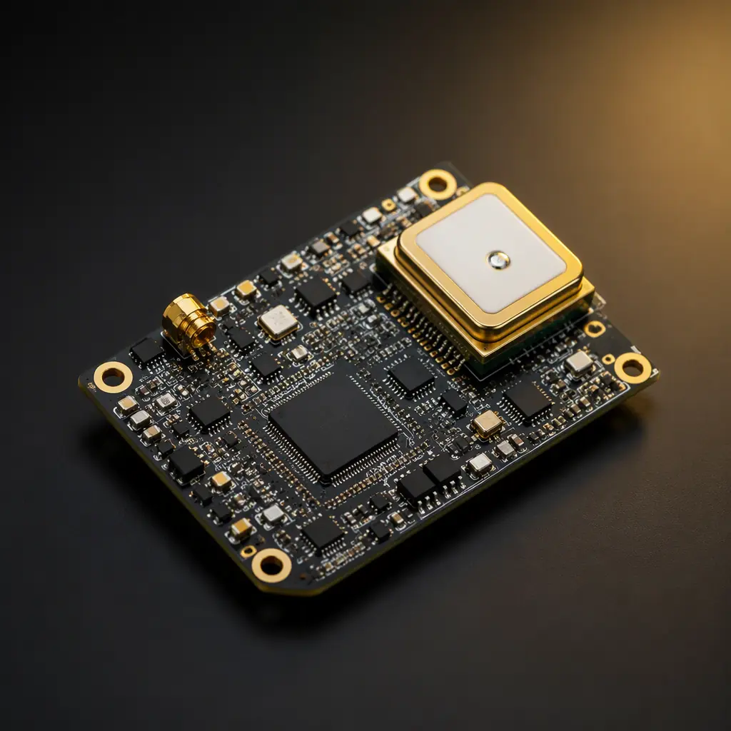
A GNSS receiver does not fail gradually — it either acquires a fix or it does not. The difference is rarely in the module datasheet; it is in the PCB that surrounds the module. The antenna feed line, the low-noise amplifier (LNA) placement, the ground plane beneath the antenna, and the shielding between the RF front end and digital noise all sit on your board, and every one of them is a decision the module vendor cannot make for you.
Huaxing PCBA builds GNSS boards for tracking devices, drone navigation, automotive telematics, and precision agriculture — up to 32 layers with ±5% impedance control, laser-drilled microvias, and 0.3 mm BGA assembly across 8 SMT lines. This guide covers the RF layout rules that determine real-world positioning performance, the manufacturing tolerances you should specify, and the assembly checks that catch problems before your product ships.
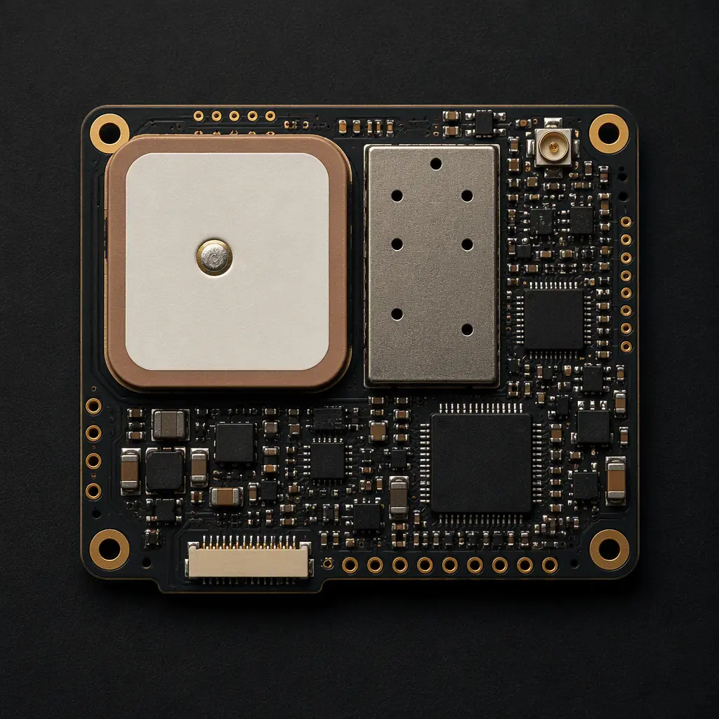
Why the Antenna Ground Plane Decides Everything
A GNSS signal at the antenna is roughly −130 dBm — a hundred million times weaker than the noise floor of a typical receiver input. The ceramic patch antenna is a half-wavelength radiator, and its ground plane is the other half of the antenna. If the ground plane is too small, has copper removed beneath the patch, or is coupled to noisy digital returns, the antenna detunes, gain drops, and the receiver needs more satellite signal to lock.
Three ground-plane rules matter more than anything else on a GNSS board:
Size the Ground Plane for the Antenna, Not the Module
Most ceramic patch antennas specify a minimum ground plane of 30–40 mm square. A tracker PCB that is only 25 mm wide cannot host a full-size patch antenna properly — the antenna's center frequency shifts and the radiation pattern tilts. Either enlarge the board, choose a smaller antenna with a documented smaller ground requirement, or move to a chip antenna with a manufacturer-defined counterpoise. Do not crop the ground plane to fit the antenna; that reverses cause and effect.
Never Remove Copper Under the Patch
The ground plane directly beneath a ceramic patch antenna is part of the radiating structure. Route no traces, place no vias, and pour no secondary fills in the region directly under the patch footprint. If the antenna sits over a split in the ground plane — for example, over a power-plane split on layer 2 — the effective antenna aperture shrinks and the resonant frequency shifts by tens of MHz, which is enough to lose the L1 band edge.
Keep Digital Noise Off the Antenna Reference
The antenna ground is also the receiver's RF reference. High-speed digital switching currents that flow through this plane couple directly into the antenna port. Stitch the antenna ground to the main ground plane at the antenna's edge with a ring of vias, and keep the digital section's return currents off this zone. Our EMC/EMI compliance guide covers plane partitioning in more depth.
Key Takeaway: The ground plane under a GNSS patch antenna is half the antenna. Size it to the antenna spec, keep copper intact beneath the patch, and isolate it from digital return currents — or no receiver design will compensate.
Antenna Feed Line: 50 Ω with the Right Launch
Between the antenna and the receiver's LNA, the feed line carries the weakest signal on the board. Every mismatch reflects energy back to the antenna; every millimeter of loss subtracts directly from link margin. A 50 Ω controlled-impedance trace is the baseline — but the details of the launch and the stackup determine whether it is actually 50 Ω across the band.
| Feed Line Element | Typical Spec | What It Protects |
|---|---|---|
| Characteristic impedance | 50 Ω ± 5% | Reflection loss at L1 (1575.42 MHz) |
| Trace width (4-layer, J=0.1 mm) | 0.35–0.45 mm | Controlled by stackup Dk and spacing |
| Feed length | < 30 mm ideal | Insertion loss — each mm adds ~0.02 dB |
| Via count on the feed | 0–1 | Each via adds ~0.1–0.3 dB and a resonance risk |
| Ground return | Coplanar GND on same layer | Confines field, blocks coupling |
If the feed must change layers, place the transition via next to a ground via so the return current has a continuous path — a missing return via turns the via into a series inductor that resonates in the L1 band. Keep the feed on the outer layer if possible; inner-layer feeds add via transitions and make impedance verification harder. When a U.FL/IPEX connector is used instead of a direct antenna, the connector's pad capacitance also needs tuning — the standard fix is a small series pad or a shortened stub in the matching network, verified with a network analyzer on the first article.
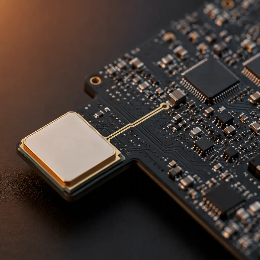
Specify impedance coupons on the panel so the fab can TDR-verify the actual feed impedance before assembly. Our impedance control guide explains the coupon design and acceptance limits, and the RF PCB manufacturing guide covers material and tolerance strategy for RF front ends.
LNA Placement: Short Feed, Clean Supply, Quiet Ground
Many GNSS modules integrate the LNA; external LNAs appear when the antenna is far from the module (active antenna) or when the module's internal noise figure is too high for the application's sensitivity budget. Wherever the LNA sits, it is the most sensitive component on the board — its placement rules are non-negotiable.
Place the LNA as Close to the Antenna Port as Possible
The trace between antenna and LNA input is where the system's noise figure is set — loss before the LNA adds directly to the noise figure. Keep this trace under 10 mm; every 0.1 dB of pre-LNA loss costs about 0.1 dB of sensitivity. If the antenna is remote (active antenna), the LNA belongs in the antenna itself and the module runs off the DC bias fed up the coax.
Give the LNA a Dedicated, Filtered Supply
LNA gain is typically 15–25 dB, so any noise on its supply is amplified straight into the receiver. Feed the LNA from a dedicated LDO or a filtered branch — a ferrite bead plus 100 nF and 1 µF decoupling, with the decoupling caps as close to the LNA pins as the footprint allows. Never share the LNA supply directly with a switching regulator output without filtering.
Guard the LNA Output and Input From Each Other
A 20 dB-gain LNA's output is a strong signal relative to its input. If output and input traces run parallel for more than a few millimeters, feedback oscillation is possible. Keep input and output traces separated by at least 3× the trace width, ideally on different routing layers, and never route them on adjacent layers without a ground plane between them.

Procurement Tip: When you send a GNSS board to fabrication, state the LNA feed-line impedance target (±5%), request impedance coupons, and ask for the measured TDR report. A fab that returns measured data instead of "designed to spec" is a fab that controls its process.
Shielding: Where the Shield Can Goes, and How It Grounds
The receiver front end needs protection from two noise sources: the board's own digital circuits (MCU, memory, switching regulators) and external interferers (cellular transmitters, Bluetooth, Wi-Fi). A shield can over the RF section is the standard solution, but only if it is designed and assembled correctly.
Define the Shield Zone in the Layout, Not After
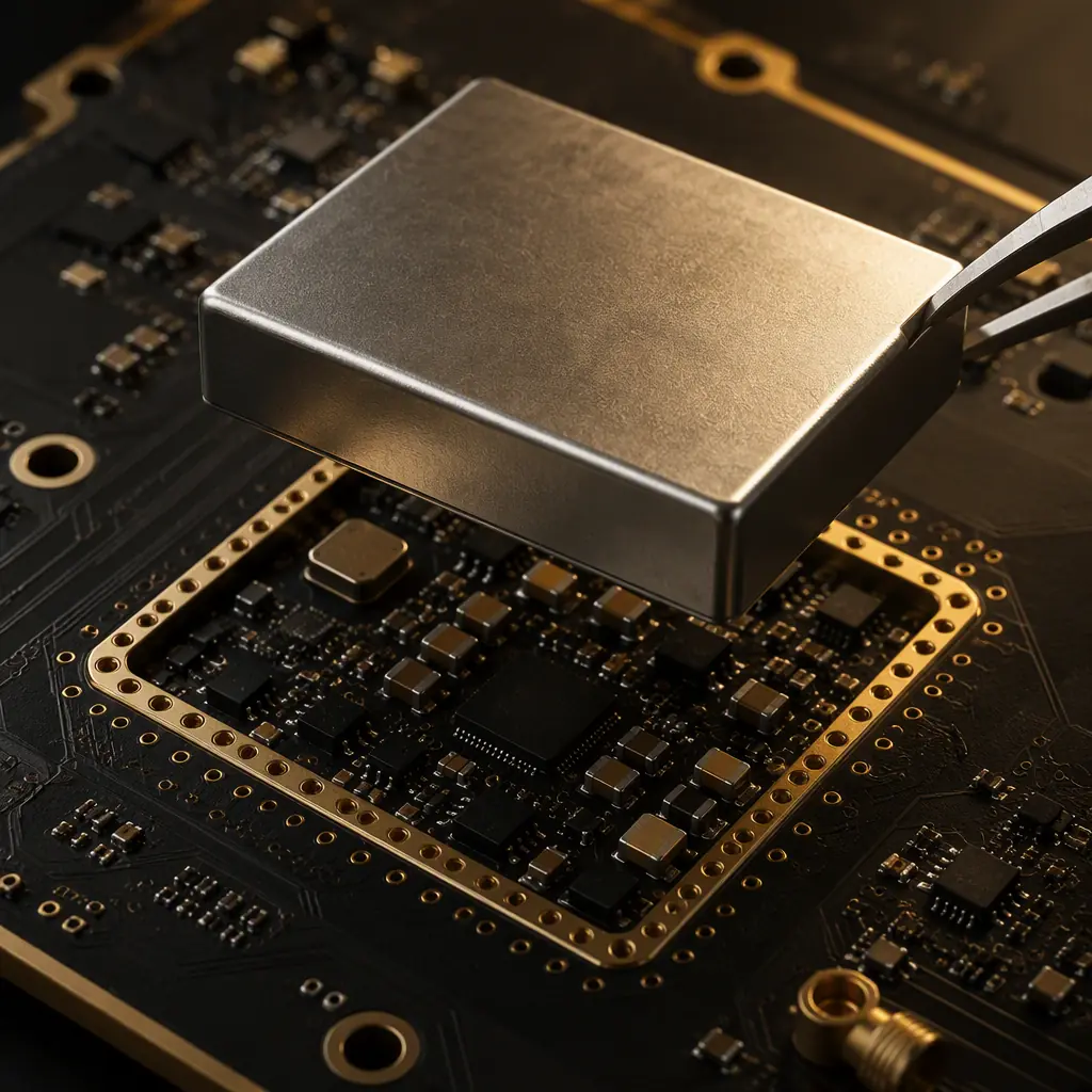
The shield fence footprint needs a continuous ground ring on the top layer, at least 1 mm wide, with vias to the internal ground plane every 2 mm or closer. A fence with sparse vias is a slot antenna at cellular frequencies — it can make interference worse. Include the fence pads in the original layout; retrofitting a shield to a finished board rarely works.
Keep the Antenna Outside the Shield
An antenna inside a shield can is detuned and desensitized — the can is a resonant cavity at L-band. The classic architecture is antenna at the board edge, RF feed entering the shielded zone through a small aperture, and everything after the matching network inside the can. If the module has an integrated antenna, the antenna must stay outside the can by definition.
Verify Shield Solder Coverage in Assembly
A shield can with a few dry joints is electrically a loose lid — it reduces shielding by tens of dB at some frequencies. Specify X-ray or AOI inspection of shield fence solder joints, and require the fence pads to have adequate solder paste volume in the stencil design. Our BGA and fine-pitch assembly guide covers X-ray verification practice that applies to shield cans too.
Stackup and Materials: FR-4 Works, With Discipline
Unlike 5G mmWave boards, GNSS at 1.5 GHz does not demand exotic laminates. Standard FR-4 has acceptable loss at L1 — the challenge is controlling the dielectric constant variation that shifts impedance. A 4-layer stackup with a solid ground plane under the RF layer is the workhorse configuration for GNSS designs.
| Stackup Choice | Best For | Trade-off |
|---|---|---|
| 2-layer, antenna on top edge | Simple trackers, lowest cost | Thin ground, feed impedance harder to hold |
| 4-layer (Sig-GND-PWR-Sig) | Most GNSS products | Good balance; keep RF on outer layer |
| 6+ layer with RF on outer | GNSS + cellular + Wi-Fi combo boards | More cost; needs isolation strategy between radios |
| Hybrid with Rogers/PTFE RF layer | Multi-band or high-precision receivers | Higher cost and lead time; needed only for extreme sensitivity |
For most products, specify FR-4 with a controlled Dk tolerance from the laminate supplier (typical ±5% on Dk) and let the fab compute trace widths for 50 Ω from the actual stackup. If you need every last decibel of sensitivity — for example, a rover-grade receiver — a hybrid stackup with a Rogers RO4003C or PTFE RF layer is justified; our PTFE high-frequency manufacturing guide covers the processing constraints (plasma treatment, drilling, plating) that hybrid boards require.
Production Testing: The Checks That Catch Bad Boards
Electrical test and AOI verify the board is assembled correctly, but neither proves the RF section works. GNSS performance depends on impedance, antenna tuning, and shielding integrity — all invisible to a flying probe. Production GNSS testing has three tiers:
Tier 1: Impedance Coupon Verification (Every Panel)
TDR-measured impedance on the panel coupons must fall inside the ±5% window before assembly. This is the cheapest RF insurance you can buy — a panel-wide impedance drift is caught here, not after 1,000 boards are in the field. Require the TDR report with your first article.
Tier 2: RF Functional Test With a GNSS Simulator
A GNSS constellation simulator injects a known signal at the antenna port and verifies acquisition time, C/N0, and position accuracy against a pass/fail mask. This catches LNA gain issues, filter problems, and feed-line faults that electrical test cannot see. For products where a missed fix is a safety issue — automotive, agricultural autosteer — simulator testing every board is the standard.
Tier 3: Live-Sky Spot Check (Sample)
A live-sky test with a real antenna confirms the complete system — antenna, feed, receiver — acquires and tracks satellites with expected C/N0 values. Sample-level live-sky testing (e.g., 5% of production) catches antenna supplier drift and assembly variations that a simulator on the bench cannot. Our testing methods guide compares RF functional test against other electrical test approaches.
Summary: The GNSS Layout Checklist
A GNSS receiver works when the RF chain is treated as one continuous structure: antenna plus ground plane, feed line with verified impedance, LNA with clean supply and short input trace, and a shield zone that is designed in from the start. Every one of these decisions is made in the layout, and every one can be verified at the factory before mass production.
At Huaxing PCBA, we manufacture GNSS boards up to 32 layers with ±5% impedance control, laser microvias, and 0.3 mm BGA assembly. Our DFM review checks antenna ground plane integrity, feed-line impedance targets, and shield fence via density before tooling. Read our RF board manufacturing guide to prepare your design, or send your files for a free DFM review and quote.
