
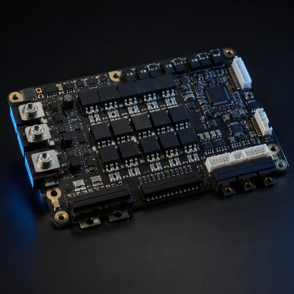
Portable power stations grew from niche camping gear into a mainstream 2026 consumer category: units from 100 Wh pocket bricks to 2,000+ Wh outdoor generators, all built around the same three power stages — a battery management system, an inverter, and a charging front end with solar input. At 1,500 W output, the battery-side current reaches 30–60 A at 24–48 V, which means the PCB design rules are closer to industrial power electronics than consumer electronics.
Huaxing PCBA manufactures power station boards for energy brands — heavy-copper BMS and inverter boards up to 6 oz copper, 16-layer stackups for the digital control sections, selective solder for through-hole power components, and UL-recognized processes for the 2026 certification cycle. This guide covers the architecture choices, the copper and thermal rules, and the certification path that determines whether your power station reaches US shelves.
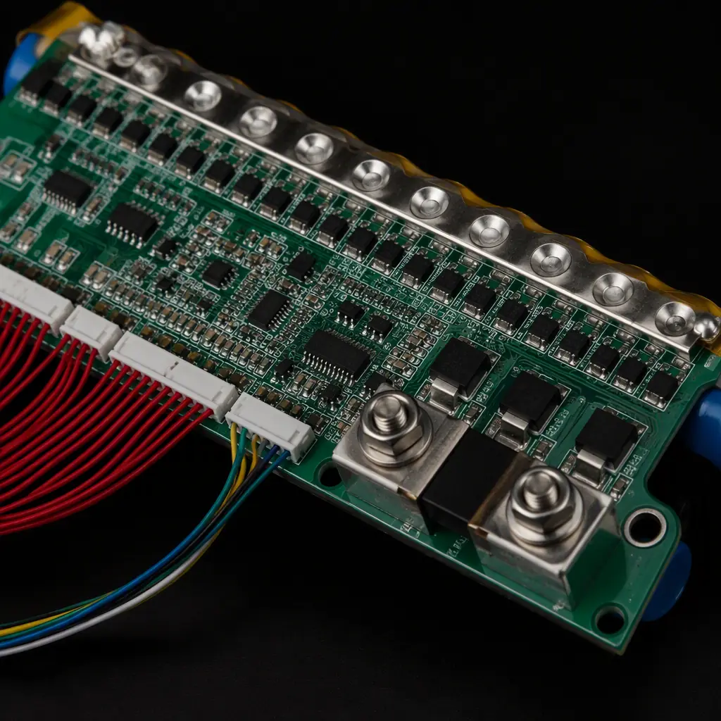
Power Station Architecture: From Cell to AC Outlet
Every portable power station is the same electrical story with different numbers: a battery pack, a protection and balancing layer (BMS), a DC bus, an inverter for AC output, and a charging front end that accepts AC, solar, and increasingly USB-C PD input. The PCB design decisions hinge on three numbers: pack voltage, inverter power, and charge power.
| Class | Capacity | Pack Config (LiFePO4) | Bus Voltage | Inverter |
|---|---|---|---|---|
| 100–300 Wh | 3S (9.6 V) – 4S (12.8 V) | 12 V | 100–300 W | |
| Mid | 500–1000 Wh | 8S (25.6 V) | 24 V | 600–1000 W |
| Large | 1500–2000+ Wh | 16S (51.2 V) | 48 V | 1500–2400 W |
The 2026 market has consolidated on LiFePO4 — roughly 3,500 cycles vs 500–800 for NMC, which is the headline spec buyers compare. The higher-voltage 48 V packs cut battery-side current dramatically (a 2,000 W inverter at 48 V draws ~45 A vs ~165 A at 12 V), which is why the large class moved to 16S. Our energy storage PCB guide covers the grid-scale version of the same architecture.
BMS Design: Balancing, Protection, and the Cell Counts
The BMS is the safety layer of the product — it is also where most certification findings land, because UL and UN38.3 look at protection behavior, not just cell quality.
Balance Current and Topology Scale With Cell Count
A 16S pack needs a 16-channel AFE with passive balancing; balance current of 100 mA is the practical minimum for a pack that sits fully charged for weeks between trips. Larger 2,000 Wh units increasingly use active balancing (inductive cell-to-cell transfer) to recover capacity from weak cells. Specify the balancing strategy in the BMS spec, and verify the AFE's measurement accuracy — a 5 mV cell-voltage error translates directly into lost usable capacity. Our EV BMS PCB guide covers AFE selection and layout.
Protection Must Be Redundant and Latching
Over-voltage, under-voltage, over-current, over-temperature, and short-circuit protection are mandatory per cell group. The critical design rule: protection must be hardware-latched, not firmware-reset — a BMS that re-enables output after a fault can turn a cell failure into a thermal event. Use a dedicated protection IC plus a secondary hardware comparator chain, and require the BMS vendor to provide fault-latch verification data. Our functional safety guide covers the independent fail-safe principle.
Current Sensing: Shunt Location and Kelvin Layout
The BMS measures pack current through a shunt resistor — typically 0.5–1 mΩ for the 50–100 A class. The shunt's sense traces must be Kelvin-connected (four-wire) directly at the shunt pads, routed as a differential pair, and kept away from the power traces. A 5 mm sense-trace detour through the power path adds an error that reads as wrong state-of-charge. Our power integrity guide covers precision sensing layout.
High-Current PCB Design: Heavy Copper, Bus Bars, and Thermal Paths
This is where portable power station boards differ from everything else in consumer electronics: the power paths carry tens of amps continuously, and the copper has to be sized like a wire, not a trace.
Size the Copper for 4× the Continuous Current
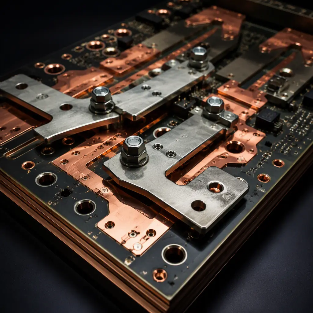
At 45 A continuous on a 48 V pack, a 2 oz trace would need to be absurdly wide; the standard solution is 3–6 oz copper on the power layers plus bus bars for the highest-current links. A 6 oz, 10 mm trace carries roughly 60 A with acceptable rise; beyond that, use a tin-plated copper bus bar bolted to the board. Our heavy copper PCB guide covers the plating, etching, and design rules for 3–6 oz layers.
Every High-Current Joint Needs a Thermal Path
MOSFETs, the shunt, and the bus-bar lands dissipate tens of watts. Each power component needs a copper island with thermal vias to an internal plane or a dedicated heatsink zone — and the enclosure needs a thermal interface to that zone. A power station that thermal-throttles on a 35 °C campsite day is a product failure. Our thermal management guide has the via-array and plane design rules.
Plan the Inverter Loop Before Layout Starts
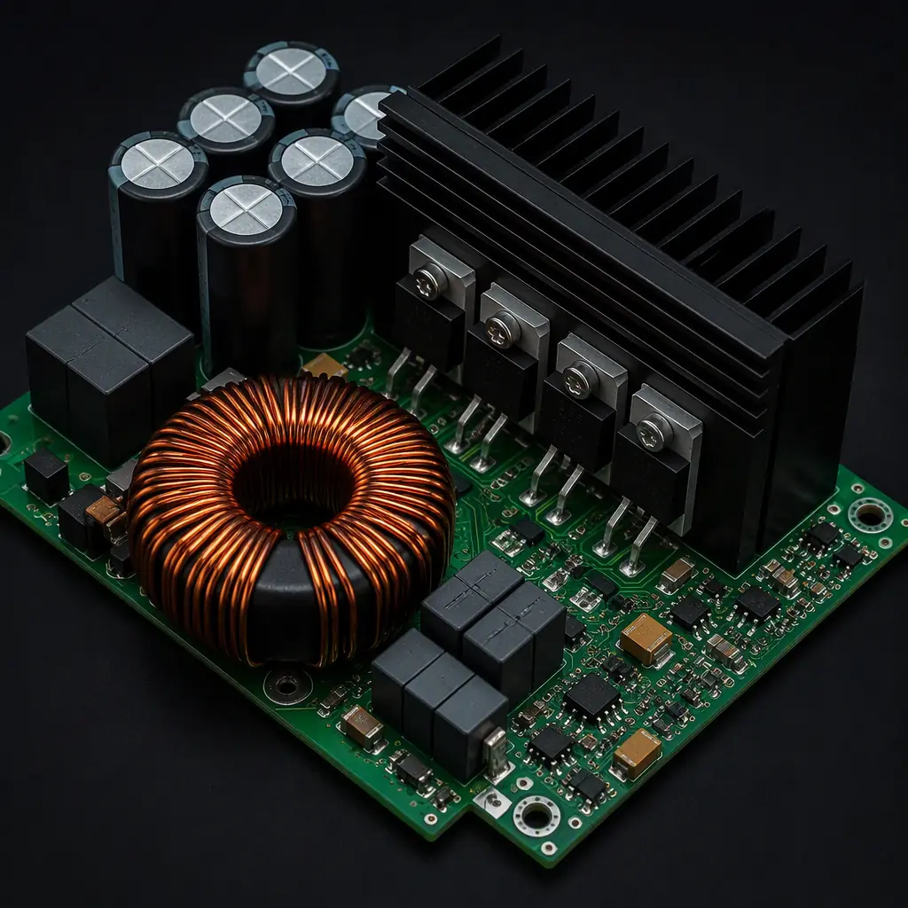
The inverter's high-frequency switching loop (DC bus capacitors to MOSFETs to transformer/inductor) must be physically small and tight — loop inductance here shows up as voltage spikes that kill MOSFETs and as radiated EMI. Put the DC-link capacitors within millimeters of the inverter MOSFETs, and keep the AC output path separate from the DC sense paths. Our power electronics guide covers inverter-stage layout in depth.
Inverter and Charging: Sine Wave, MPPT, and GaN Fast Charge
The output stage and the input stage are two different power electronics problems sharing one board.
Pure Sine Wave Is Table Stakes — THD Below 3%
Every 2026 power station advertises pure sine wave output; buyers running CPAP machines, induction cooktops, and power tools check the spec. Target total harmonic distortion below 3% at rated load and verify output waveform on the functional test line with a resistive and a motor load. The inverter control loop and the output filter (LC) dominate THD — specify the filter design in the DFM review. Our solar inverter guide covers the grid-tie variant of the same stage.
MPPT Input: Design for the Panel Voltage Range, Not the Label
Solar input is nominally 12–48 V, but open-circuit voltage runs ~20% higher than the label. The MPPT front end must survive the full Voc range plus cold-temperature spikes, and the input connector needs reverse-polarity protection (solar cables get swapped). Specify MPPT efficiency ≥ 98% at the design review and verify it on the production test with a solar simulator. Our new energy PCB guide covers the input-stage protection requirements.
GaN Fast Charge: 100 W USB-C PD Is Now Standard
Flagship units charge at 100 W over USB-C PD and 500–1000 W from AC. GaN (gallium nitride) FETs in the AC charger stage run at 100–300 kHz switching frequencies, which shrinks magnetics but demands careful layout — tight gate loops, low-inductance source connections, and thermal management for the GaN parts. If your design uses GaN, the layout rules are stricter than silicon; budget for a layout review pass. Our thermal management design guide covers the power-component layout rules.
Thermal Management and Enclosure Integration
A power station is a sealed box with a battery and an inverter inside — the thermal budget has to be designed as a system, with the PCB as the primary heat spreader.
Model the Worst-Case Corner: Full Inverter + Full Charge in 40 °C
The design thermal case is not "nominal use" — it is a customer charging at full AC rate while running the inverter at rated load in a hot vehicle. Model that corner in the design review: total dissipation of 30–60 W is typical for a 1,500 W unit, and the PCB thermal vias and enclosure fins have to move it out. Our thermal management guide has the via-array sizing methodology.
Put Thermal Sensors on the Copper, Not Just the Air
BMS over-temperature protection should read the cell and board temperature, not the ambient. Place NTC sensors on the BMS board near the MOSFETs and shunt, with thermal vias under the sensor pads so they track the copper temperature quickly. A slow thermal sensor turns a momentary overload into a battery event. Our thermal cycling guide covers sensor placement practice.
Safety and Certification: UL 2743, UN38.3, and the 2026 Market
Portable power stations are among the most certification-heavy consumer products in electronics. The certification strategy should shape the PCB design from the first layout pass.
UL 2743 Is the North American Gate
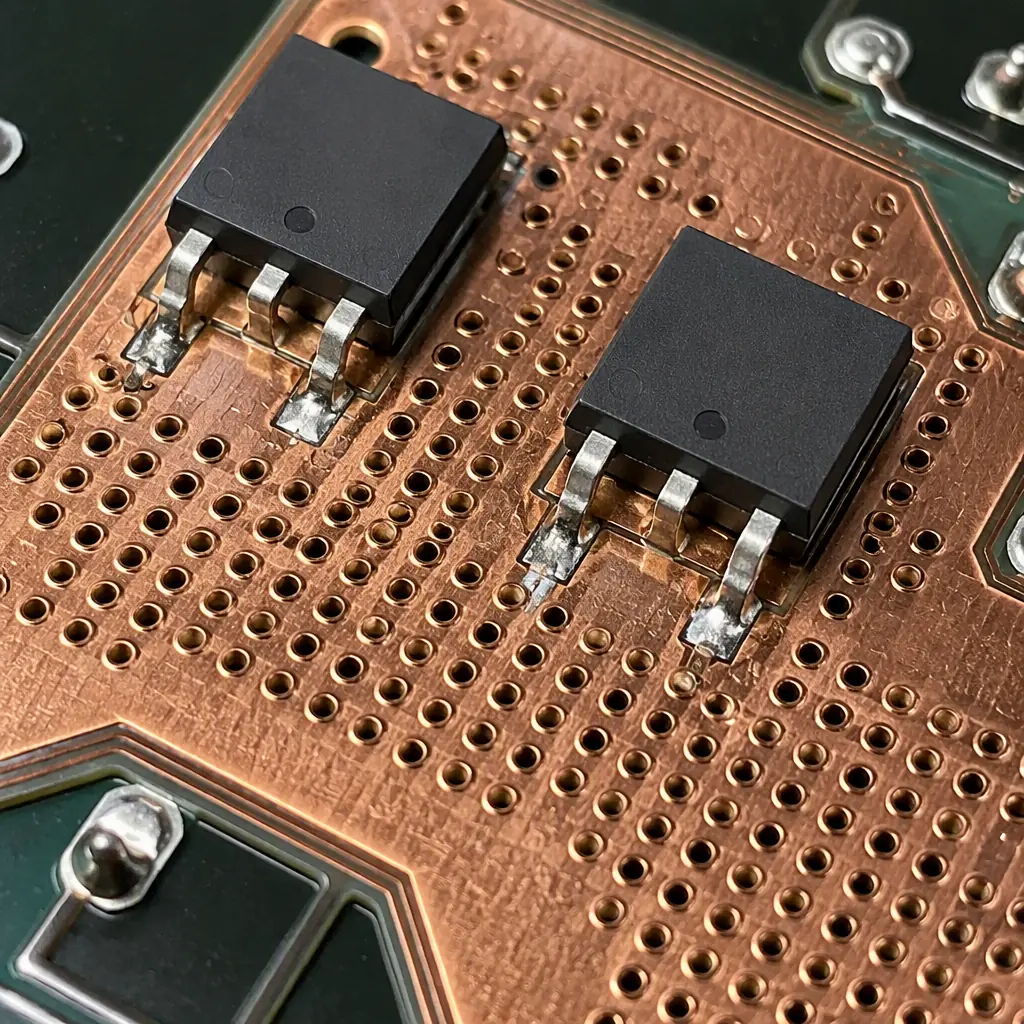
UL 2743 (Portable Power Packs) covers the whole unit — battery, inverter, charger, enclosure. The standard's requirements include fault tests that the PCB must survive: component-level failures must not lead to fire or electric shock. Design for UL from the start: trace spacing per working voltage, fuse protection on every output, and documented component ratings. Our UL certification guide covers UL 796 and the board-level requirements.
UN38.3 Is About the Battery, But the Board Signs It
UN38.3 (transport of lithium batteries) requires the pack — including its BMS — to pass mechanical and electrical abuse tests. The BMS board must survive vibration, shock, and temperature cycling without the protection circuits degrading. The PCB qualification test matrix should mirror the UN38.3 profiles. Our vibration and shock testing guide has the JESD22 and MIL-STD profiles.
FCC Part 15B and the Inverter's Emissions Budget
The inverter's 20–50 kHz switching and the GaN charger's 100–300 kHz switching both radiate. Plan the emissions budget with 6 dB of margin, keep the switching loops tight, and budget for a pre-compliance scan with the inverter under load before the formal test. Our EMI/EMC guide covers switching-power emissions control.
Assembly Considerations for High-Power Boards
Heavy-copper boards and mixed through-hole/SMT assemblies need a manufacturing line that handles both — and the test strategy has to verify power behavior, not just connectivity.
Heavy Copper Changes the Fabrication and Assembly Rules
6 oz copper doesn't etch or solder like 1 oz: minimum trace/space relaxes, drill registration tolerances widen, and the reflow profile needs adjustment for the thermal mass. Confirm your fabricator's heavy-copper capability matrix before design freeze — a 3 oz minimum-space spec that the fab can't hold is a re-spin. Our manufacturing tolerances guide covers the heavy-copper deltas.
Selective Solder for the Power Components
Through-hole MOSFETs, bus-bar lands, and connector pins on heavy-copper boards should be selective-soldered rather than hand-soldered — consistent joints, repeatable fillets, no cold joints on a 45 A path. Specify selective solder with X-ray sampling on the power joints. Our wave vs selective soldering guide covers the process choice.
Functional Test With Real Power, Not Just Signal
The production test must verify the BMS protection thresholds (OVP/UVP/OCP trip points), inverter output voltage and frequency, MPPT tracking, and charge current — under load. A functional test with an electronic load and a battery simulator catches what flying probe cannot: a protection chain that trips 200 mV late. Our test method guide explains the three-tier strategy.
Summary: The Portable Power Station PCB Checklist
A power station that ships to US shelves in 2026 is a heavy-copper power board with a redundant, latched BMS; bus-bar-class current paths sized at 4× continuous; a sine-wave inverter with THD under 3%; an MPPT front end built for real panel voltages; GaN charging laid out with silicon-grade discipline; and a UL 2743 / UN38.3 certification plan that shaped the layout from day one. The PCB copper is where the power density lives — everything else is packaging around it.
At Huaxing PCBA we manufacture portable power station BMS and inverter boards up to 6 oz copper with selective solder, 100% flying probe, and functional test with electronic loads and battery simulators. Our DFM review checks copper sizing, inverter loop inductance, BMS fault-latch design, and certification spacing before tooling. Read our energy storage guide to prepare your design, or send your files for a free DFM review and quote.
