
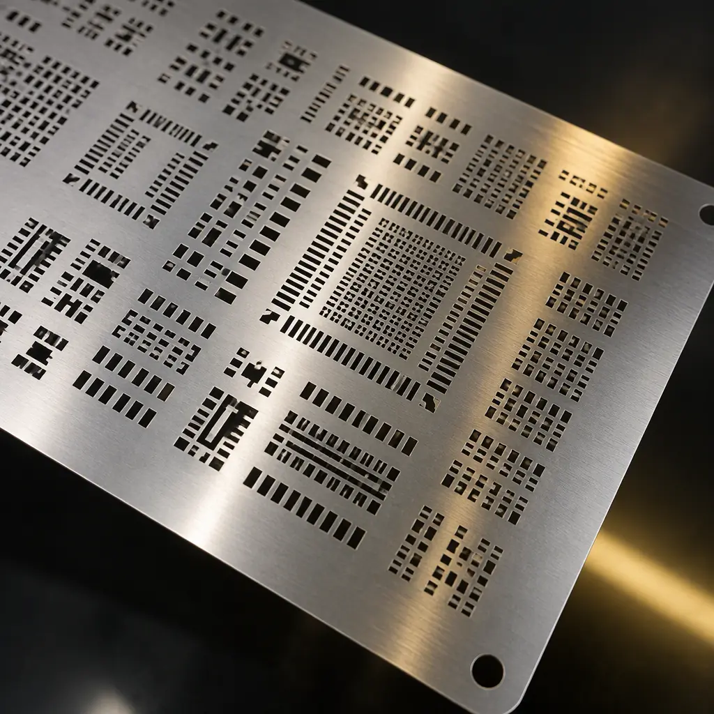
When an assembly line reports insufficient solder, the instinct is to blame the printer settings. In a large share of cases the printer is doing exactly what the stencil geometry allows it to do — and the geometry was decided weeks earlier, on a CAD station, without anyone running the arithmetic. Aperture design determines the ratio of aperture wall area to aperture opening area, and that ratio determines how much solder paste adheres to the stencil wall instead of transferring to the pad.
This guide sets out the mechanics of paste release, the two ratios that govern it, the step-stencil and overprint techniques that recover volume where the ratio cannot be met, and the aperture specification a buyer should insist on in the stencil purchase order. The numbers matter: a printed deposit that is 25 percent short of nominal volume will produce a joint that passes visual inspection and fails thermal cycling. At Huaxing PCBA, stencil design is reviewed at DFM stage against the area-ratio arithmetic below before a laser-cut foil is ordered.
The Physics: Why Paste Sticks to the Stencil Wall
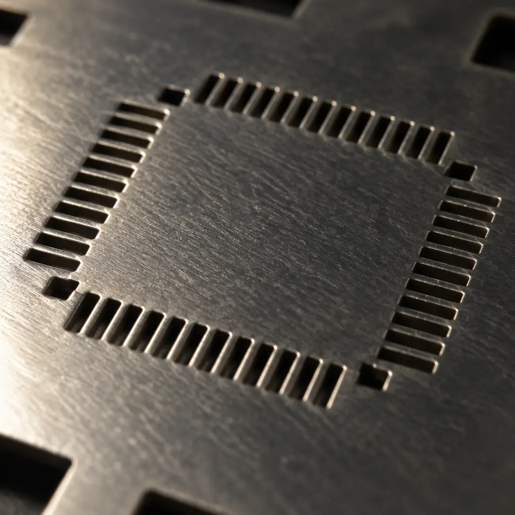
Solder paste does not fall out of an aperture. It is transferred. During the print stroke it is pressed into the aperture, and during stencil release the newly formed deposit must separate from two surfaces: the pad below it, where adhesion is desirable, and the aperture wall around it, where adhesion is a defect.
The share of paste that stays with the stencil wall is governed by the competition between three forces: adhesion of the paste to the pad, adhesion of the paste to the aperture wall, and the cohesive strength of the paste itself. The paste-to-wall adhesion scales with the wall surface area in contact with the paste, which is the aperture perimeter multiplied by foil thickness. The paste-to-pad adhesion scales with the aperture opening area. The ratio of the second to the first is the area ratio, and it is the single most useful number in stencil design.
Key Takeaway: Area ratio = (aperture opening area) ÷ (aperture wall area), where wall area = aperture perimeter × foil thickness. The industry threshold for reliable release on a rectangular aperture is AR ≥ 0.66, with 0.70 or better preferred for aperture fill areas above roughly 80 percent of the pad. Below 0.60, transfer efficiency falls off a cliff rather than degrading gently.
Working the Arithmetic for Common Geometries
The two ratios are computed differently for rectangular and circular apertures. Rectangular apertures use area ratio (opening area ÷ wall area). Circular apertures use aspect ratio — aperture diameter ÷ foil thickness — with a threshold of 1.5:1 rather than 0.66.
| Foil Thickness | Aperture (W × L) | Area Ratio | Expected Transfer Efficiency | Typical Application |
|---|---|---|---|---|
| 0.12 mm (5 mil) | 0.50 × 0.55 mm | 0.90 | 90–100% | 0201/0402 passives, 0.5 mm pitch |
| 0.12 mm | 0.30 × 0.35 mm | 0.64 | 70–85% | 01005 passives, 0.4 mm pitch |
| 0.15 mm (6 mil) | 0.25 × 0.25 mm | 0.42 | Below 50% — not viable | Requires step-down before printing |
| 0.10 mm (4 mil) | 0.25 × 0.30 mm | 0.68 | 80–95% | Fine-pitch QFP, 0.4 mm pitch |
| 0.08 mm (3 mil) | 0.20 × 0.25 mm | 0.69 | 80–95% | 0.35 mm pitch, package-on-package |
| 0.12 mm | Ø 0.25 mm circle | AR 0.52 / aspect 2.08 | Acceptable by aspect ratio | Microvia fill, small round pads |
| 0.15 mm | Ø 0.20 mm circle | AR 0.33 / aspect 1.33 | Marginal — below 1.5 aspect | Requires foil reduction to 0.12 mm |
The table shows the central design conflict. Bulk solder volume for through-hole, connector and power pads scales with foil thickness, so thicker foils are attractive. Fine-pitch component release scales inversely with foil thickness, so thin foils are required. A single uniform foil cannot serve both die areas on a modern mixed-technology board, which is why step stencils are standard rather than exotic. The footprint side of the same problem — how pad dimensions drive deposit volume targets — is covered in our guide to IPC-7351 land pattern density levels.
Aperture Geometry Rules Beyond Area Ratio
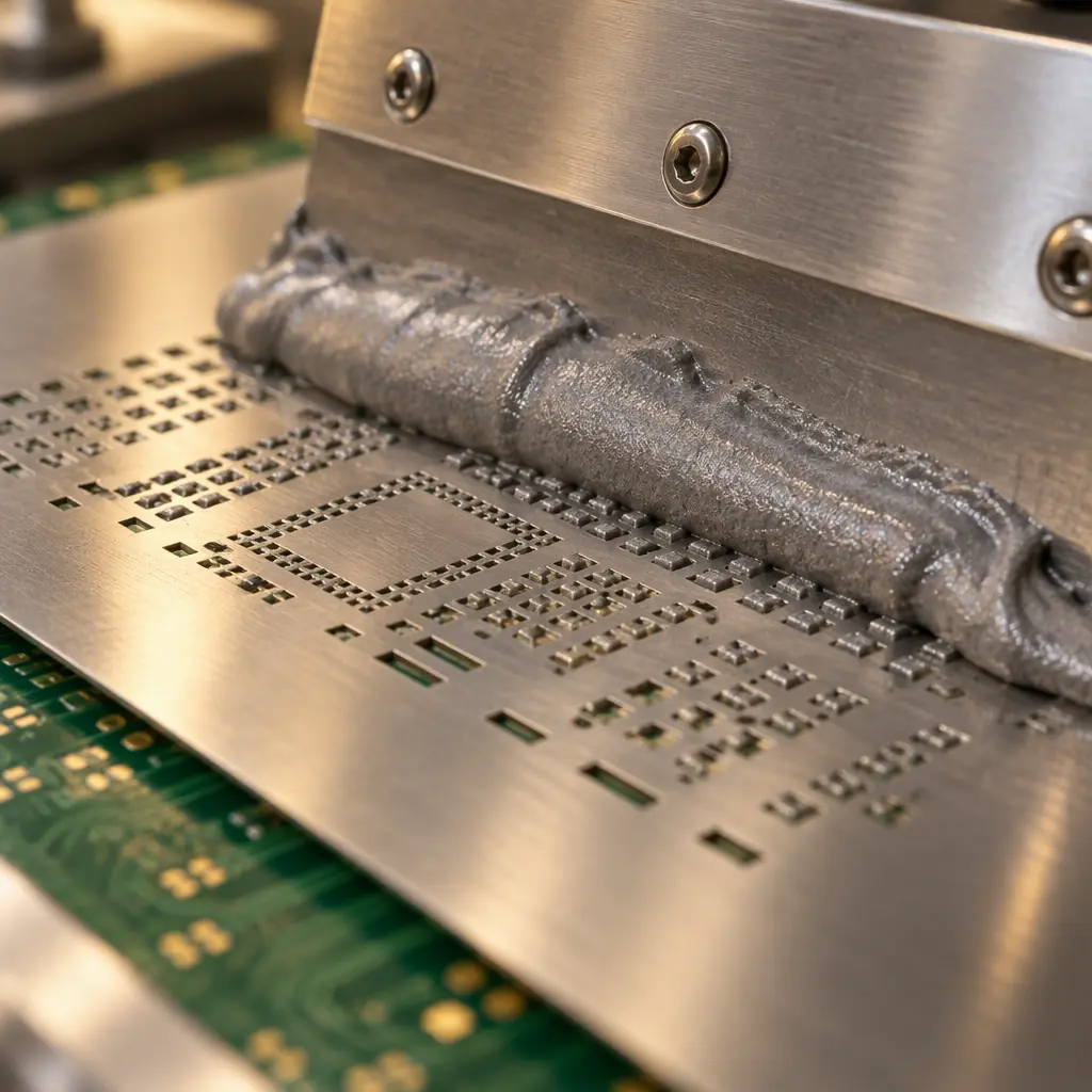
Area ratio is necessary but not sufficient. Six shape rules determine whether a compliant aperture still produces a good deposit.
Home plate shape for fine-pitch and small passives
Truncating the inner corners of a rectangular aperture — the classic home-plate or pentagon shape — reduces the aperture area slightly while shortening the wall perimeter available to hold paste. Nets: area ratio improves for the same printed volume target, because less paste is left on the wall. The corner truncation is typically 10 to 25 percent of the aperture width, applied at the two corners facing the direction of squeegee travel.
Aperture area ratio to pad, not aperture corners untouched
Aperture area is normally 80 to 100 percent of the pad area for SMT pads, and the apertures should be centred on the pad. Where a pad is connected to a large copper pour with thermal vias, the deposit tends to wick into the via barrels during reflow, so the aperture is deliberately enlarged by 10 to 20 percent to compensate. The via treatment itself is covered in filled via and via-in-pad guidance.
Separate apertures for thermal pads, windows plus spokes
A single large aperture over a QFN thermal pad produces voiding and solder beading. The standard treatment is a windowpane array: the pad is divided into a grid of smaller apertures sized to keep each individual area ratio inside the compliant band, which reduces voiding substantially. Paste coverage on the thermal pad is typically held between 50 and 80 percent of the pad area. The assembly side of the same package is covered in our guide to QFN and LGA leadless package soldering.
Aperture lengthwise extension for wave-soldered and glue-dot processes
Where a component will later pass through wave or selective soldering, the aperture is extended lengthwise by 0.2 to 0.3 mm on the trailing side to leave a solder thief. Overlapping the deposit under the body is avoided, and the extension direction follows the board travel direction. Related guidance on the process side is in wave versus selective soldering.
Aperture-to-aperture web minimum
The web of stainless steel between neighbouring apertures must be thick enough to survive the print stroke and to avoid paste bridging between adjacent pads. A practical minimum for laser-cut stainless foil is about 0.10 mm for a 0.12 mm foil, and the web should not fall below roughly 0.8 times the aperture width on fine-pitch devices. Where the web requirement and the aperture area requirement conflict, the correct resolution is to relax the aperture width, not to accept a web that will deform.
Fiducial and tooling apertures as process geometry
Stencil fiducials must match board fiducials for print alignment, and the stencil needs its own tooling apertures for the printer frame. Where board fiducials are placed too close to the panel edge, print registration drifts across the panel. Fiducial placement rules are set out in PCB fiducial mark design.
Step Stencils and Overprint: Recovering Volume Without Hurting Release
Where a board carries both fine-pitch devices and high-volume pads, a stepped foil solves the conflict by changing foil thickness locally. Three techniques are in routine use.
| Technique | How It Works | Where It Applies | Constraint to Specify |
|---|---|---|---|
| Step-up (thicker local region) | Additional foil laminated over the base foil in the high-volume area | Connectors, power pads, press-fit, through-hole | Step boundary must sit at least 2 mm from fine-pitch apertures; step height tolerance ±0.01 mm |
| Step-down (thinner local region) | Base foil thinned by etching or laser in the fine-pitch area | 0.3–0.4 mm pitch QFP, CSP, 01005 passives | Step-down depth per step ≤ 0.04 mm; multiple steps rather than one deep step |
| Overprint | Standard foil thickness with aperture area extended beyond the pad | Thermal pads, RF shields needing extra paste | Aperture must not exceed 0.2 mm beyond pad edge to avoid beading |
The constraint that causes most trouble is the step boundary position. A step edge near a fine-pitch aperture changes the effective foil thickness the squeegee sees, which produces a local paste volume gradient and a band of marginally short deposits. Requiring a 2 mm keep-out at the step boundary removes the effect at the cost of a slightly larger board area with uniform thickness.
Coating, Tension and the Stencil Order Specification
Two non-geometric properties matter as much as the aperture drawing, and both belong on the purchase order rather than in a supplier's default.
Anti-stick coating. Nano-coating the aperture walls and the foil underside reduces paste-to-wall adhesion directly, effectively raising the usable area-ratio floor. Reported gains in transfer efficiency for 01005 and 0.3 mm pitch apertures are in the 10 to 20 percent range, which frequently converts an aperture that would print at 65 percent efficiency into one that holds 85 percent. For fine-pitch production, specify nano-coating explicitly; an uncoated foil is not equivalent.
Mesh and tension for framed stencils. For a framed assembly, the foil is bonded to a tensioned mesh. Tension determines how well the foil hugs the board during the print stroke and separates on release. A typical specification is 35 to 50 N/cm initial tension, and a framed stencil should be retired when tension falls below about 30 N/cm, because a slack foil produces deposits that vary with position on the panel. Tension is a consumable property and should be measured, not assumed.
Procurement Tip: The stencil specification on a production board should name six things: foil thickness by region, coating type, area ratio for the tightest aperture with the calculation shown, step map with boundary keep-outs, mesh tension at delivery, and the laser-cut edge quality class. Suppliers who accept a bare "fine pitch" instruction will deliver whatever geometry their default library produces, and the print defects will appear on your line, not theirs.
Aperture Design Is a Yield Lever, Not a Detail
The connection between aperture geometry and line performance is direct and measurable. Where area ratio falls below the threshold, transfer efficiency drops, deposits are short, and the downstream defects follow in a predictable order: insufficient solder on fine-pitch terminations, then open joints after thermal cycling, then head-in-pillow on area-array packages where the paste column cannot bridge the warped gap. Each of those defects has a distinctive signature, covered in our guide to tombstoning and head-in-pillow defects.
Because the geometry is fixed before the first board is printed, an aperture review at DFM stage is the cheapest yield intervention available on a new product. Changing a stencil after tooling costs a foil and a print study; changing the deposit volume after ramp costs production output. The statistical side of holding that volume in control is described in solder paste volume and SPI process control, and the defect patterns that print settings can and cannot fix are covered in solder paste printing defects.
Summary
Solder paste release is a geometry problem with a numeric answer. Area ratio determines how much paste the stencil gives back, and the 0.66 threshold is the practical floor below which deposits become unreliable regardless of printer settings. The rest of aperture design — home plate corners, thermal pad windows, web minimums, step maps and coating — exists to hold that ratio in a compliant band while meeting the volume demands of the mixed-technology board.
For the buyer, the useful move is to require the ratio to be shown. A stencil supplier asked to document area ratio for the tightest aperture on the board will either produce a compliant calculation or reveal that the design needs a foil change or a step before production starts. Both outcomes are cheaper than discovering it from a yield report.
At Huaxing PCBA we review every new assembly's stencil geometry at DFM stage, compute area ratio for the tightest aperture, and specify step maps, coating and tension on the stencil purchase order. We run SPI on all eight SMT lines so printed volume is measured per pad rather than inferred. Review our fine-pitch assembly guide or contact our engineering team with your stencil and paste requirements.
