

Leadless packages, QFN (Quad Flat No-leads), DFN, LGA (Land Grid Array) and the SO-8/power variants that share their construction, have become the default for anything compact. There are no gull-wing or J-shaped leads, so the package is smaller, the thermal resistance is lower, and the part can be placed at very fine pitch. That is exactly why they show up in wearables, IoT modules, motor drives, power stages and just about every board that is tight on space. But the same geometry that makes them attractive also makes them the hardest package to solder reliably. The pad is underneath the package, the joint is not visible after reflow, and the large central thermal pad is a magnet for voiding. At Huaxing PCBA we run 8 SMT lines at 8M placements/day, handling 0201 and 0.3 mm pitch parts in a 15,000 m² facility serving 30+ countries, with leadless packages a routine part of the mix.
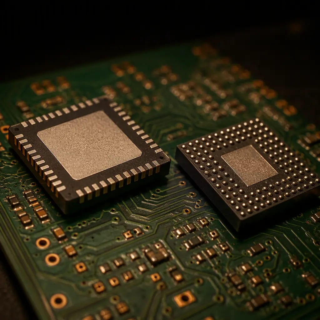
Why Leadless Packages Are Everywhere
A QFN puts the interconnect on the bottom of the package, as a perimeter of terminals around a central exposed pad. An LGA does the same but with a full or partial grid of land pads instead of a perimeter ring. Either way the package height drops, the board area shrinks and the thermal path from the die to the PCB becomes short. Which is why a leadless part can carry far more current than an equivalent leaded part of the same footprint. The trade-off is that you can no longer inspect the joint with your eyes, and the central pad behaves very differently from a peripheral terminal, so it has to be treated that way in the process.
We build these boards on the same lines that run 0.3 mm pitch BGAs and 0201 passives, so the equipment is not the constraint. The constraint is understanding that a leadless package is two different soldering problems on one part: one for the perimeter, one for the pad.
The Exposed Thermal Pad, Where Most Failures Start
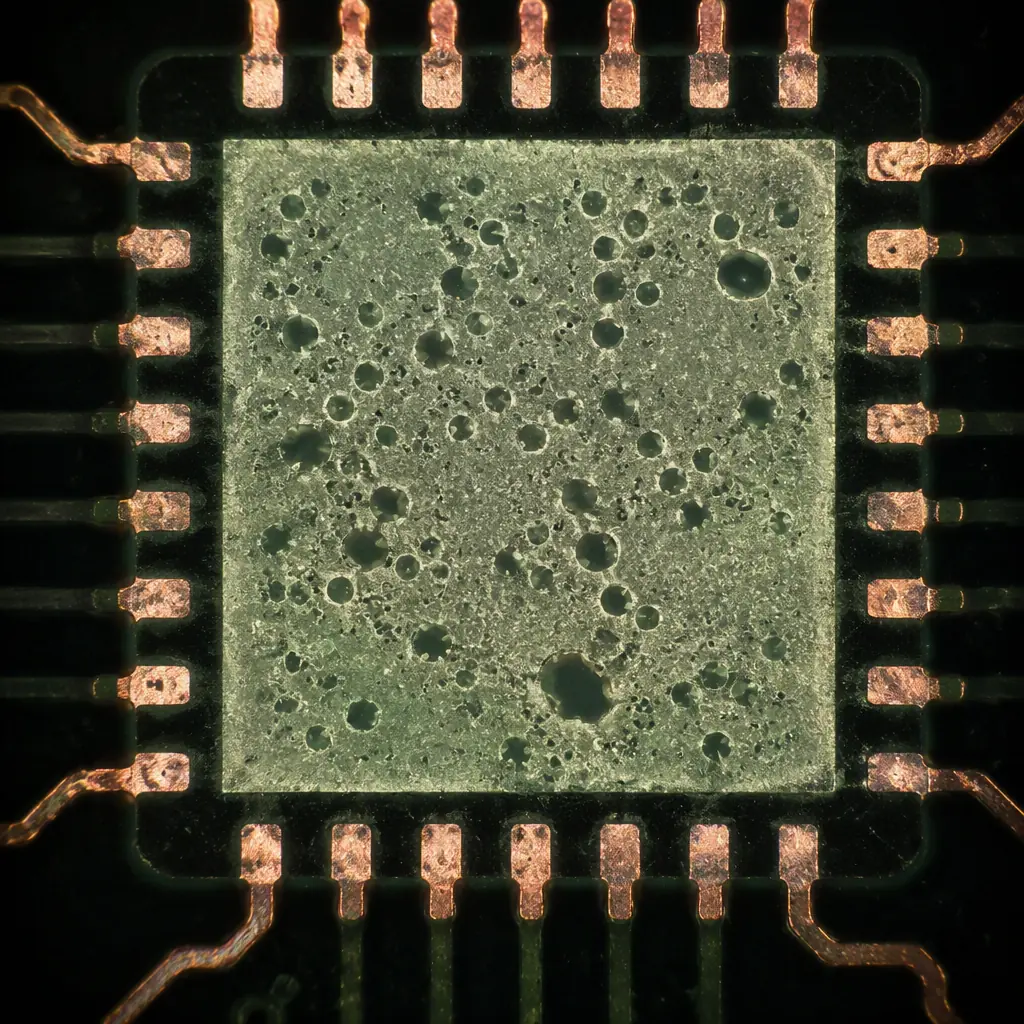
Almost every QFN and LGA has a single large exposed pad in the center. It is typically the component’s heat sink and often its ground return, so it has to make a good solder joint to the board. Because it is large and flat, the paste printed under it is prone to trapping volatiles and air, and when the solder melts the gas has nowhere to escape except to form voids. Large voids under the pad mean three problems: poor heat transfer, a high-resistance electrical connection, and a weak point that can crack under thermal cycling.
Void migration and the outgassing problem
Flux volatile and air bubble to the surface as the solder melts. In a narrow perimeter joint there is room for them to escape; under a wide pad they get trapped and form voids that often migrate to a corner or an edge. The bigger the pad, the harder it is to control. This is a print-and-reflow problem, not a placement problem.
Thermal and electrical effect
A voided pad has less metal in contact, so the thermal resistance to the board rises and the pad runs hotter. That shortens the life of the die and, for a power part, can push the junction above its limit. For a ground pad it also raises the impedance of the return path. See our thermal management and trace current capacity guides for how this plays out downstream.
The crack path
Voids create a stress raiser where the remaining solder is thinnest. Under thermal cycling a void near the pad edge can grow into a crack and eventually an open or a high-impedance joint. This is why void acceptance is a real spec, not a nicety.
Stencil Aperture Design for QFN and LGA
The single most effective lever for controlling voiding on a leadless pad is the stencil aperture that prints the paste. You do not want to flood the pad and trap gas; you want to print enough paste to make a strong joint while leaving an escape path for the volatiles. IPC-7525 guidance and practical experience both point to a coverage of roughly 50–80% of the pad area, achieved with either a window-pane (grid) aperture or a smaller aperture that still wets the whole pad.
| Aperture type | Coverage | Effect on voiding | When to use |
|---|---|---|---|
| Window-pane (grid) | ~60–75% | Lowest voiding, channels for gas | Large thermal pads >5 mm |
| Full aperture | 100% | Highest voiding unless reflow tuned | Small pads, low failure risk |
| Small offset aperture | ~50–60% | Low voiding, less solder volume | Paste-volume-sensitive design |
The perimeter terminals are a separate print, usually covered 100% of the pad. The problem is the combination . You need enough paste on the periphery for a good fillet while not over-printing the center. We set apertures per part with the stencil design documentation and validate on first article. See our fine-pitch SMT guide for how this applies as pitch shrinks.
Reflow, Flux and Wetting for Leadless Parts
Once the aperture is right, the reflow profile has to actually melt the solder fully and release the volatiles before solidifying. A common miss is a peak temperature that is barely at the paste alloy’s liquidus, leaving thick, high-void joints; another is an aggressive soak that bakes the flux before it can do its work.
Peak temperature and time above liquidus
The joint needs enough time above the alloy liquidus for the solder to fully coalesce and the gas to escape. For SAC305 that typically means a peak around 245–250°C with a healthy dwell. See our reflow profile optimization guide for the full setup.
Flux chemistry
A no-clean paste with the right activity level and a profile that lets it wet is critical. Under a large pad the flux has to move the gas out; an over-aggressive soak can leave unactivated flux and residue. Pick the paste for the package, not the line average.
Wetting on the pad
The pad finish matters. ENIG and immersion silver wet differently than bare copper, and the exposed copper pad for a leadless part has to be clean. Check our surface finish selection and solderability testing guides for finish-driven wetting issues.
The flux-residue and cleaning trade-off
Under a leadless pad, flux residue is sealed in and harder to clean. If the application needs a clean board, that changes the paste and the cleaning process. See aqueous vs solvent cleaning and ionic contamination testing.
IPC-7093 Void Criteria and X-Ray Acceptance
Because the joint is not visible, x-ray is the only reliable way to verify a leadless pad. IPC-7093 is the standard that defines design and assembly of leadless (QFN/LGA/DFN) packages, and it sets expectations for voiding and inspection. In practice, void acceptance depends on the class of the board and the function of the pad.
| Class / pad role | Typical target | Inspection method |
|---|---|---|
| Class 3 (high-reliability) power pad | ≤10% void, no large single void | Digital X-ray |
| Class 2 (standard) power pad | ≤25% void | Digital X-ray |
| Perimeter terminal | Full fillet, no open | AOI + X-ray |
The key is that tolerance is set before production, not discovered on the first bad batch. We X-ray sample leadless joints per lot and reject a panel that drifts past the agreed threshold, and we record the void percentage on the inspection report so you can see it, not just trust it. See our inspection methods and testing methods guides for how X-ray, AOI and SPI fit together.
Rework and Replacement of a Leadless Part

When a leadless part does fail, removing and replacing it is harder than a leaded part. You have to heat the whole footprint without cooking the neighbors, lift the part, clean the pad, and reprint. The risk is pad damage or thermal distortion. Use a hot-air rework station with a bottom heater and a profile matched to the part, and expect to X-ray the replacement joint, not just eyeball it. See our rework & repair guide and BGA assembly guide for the tooling and profile detail.
Procurement Tip: Ask the supplier for the IPC-7093 void target they run to on leadless parts and the X-ray sampling rate they use on your lot, and for the void percentage figure on the inspection report. A line that tells you "we X-ray check QFN" but cannot quote a void limit is telling you they do not control the one thing that fails.
What to Specify With a PCBA Supplier
Leadless packages are bought on repeatability, not on a placement spec. The table below is the practical minimum to demand when you source a board with QFNs or LGAs.
| Specification | What to demand | Why it matters |
|---|---|---|
| Stencil aperture | Window-pane or optimized aperture, 50–80% coverage | Controls voiding at the pad |
| Void limit | Class-dependent %, agreed before production | Defines a measurable reject |
| Inspection | X-ray sample + 100% AOI | Catches open, bridging, void drift |
| Reflow | Profile matched to the part, soaked for outgassing | Kills the void its own root cause |
| Rework | Hot-air station, profile documented, post-rework X-ray | Protects the board if a part is replaced |
At Huaxing PCBA we run 8 SMT lines, 4 DIP lines and 8M placements/day, with 0201 / 0.3 mm pitch capability and 32-layer fabrication, in a 15,000 m² facility with 500+ staff serving 30+ countries. We are ISO 9001, IATF 16949 and UL (E354321) certified, with 99.2% on-time delivery and 98.7% first-pass yield, and we build to IPC-A-610 Class 3 where the application needs it. Upload your design for a quote or talk to our engineering team about your leadless-package project. For related reading, see our PCB assembly process and solder joint defects guides.
