
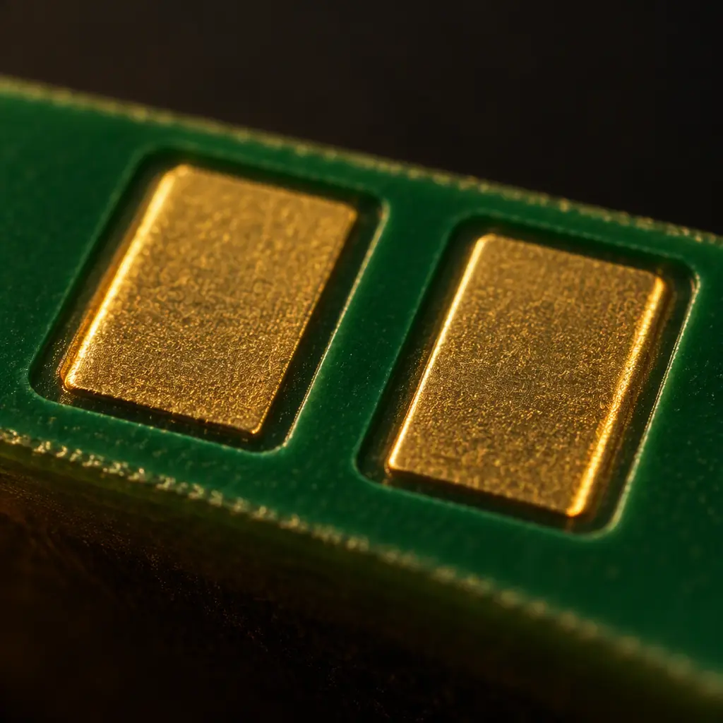
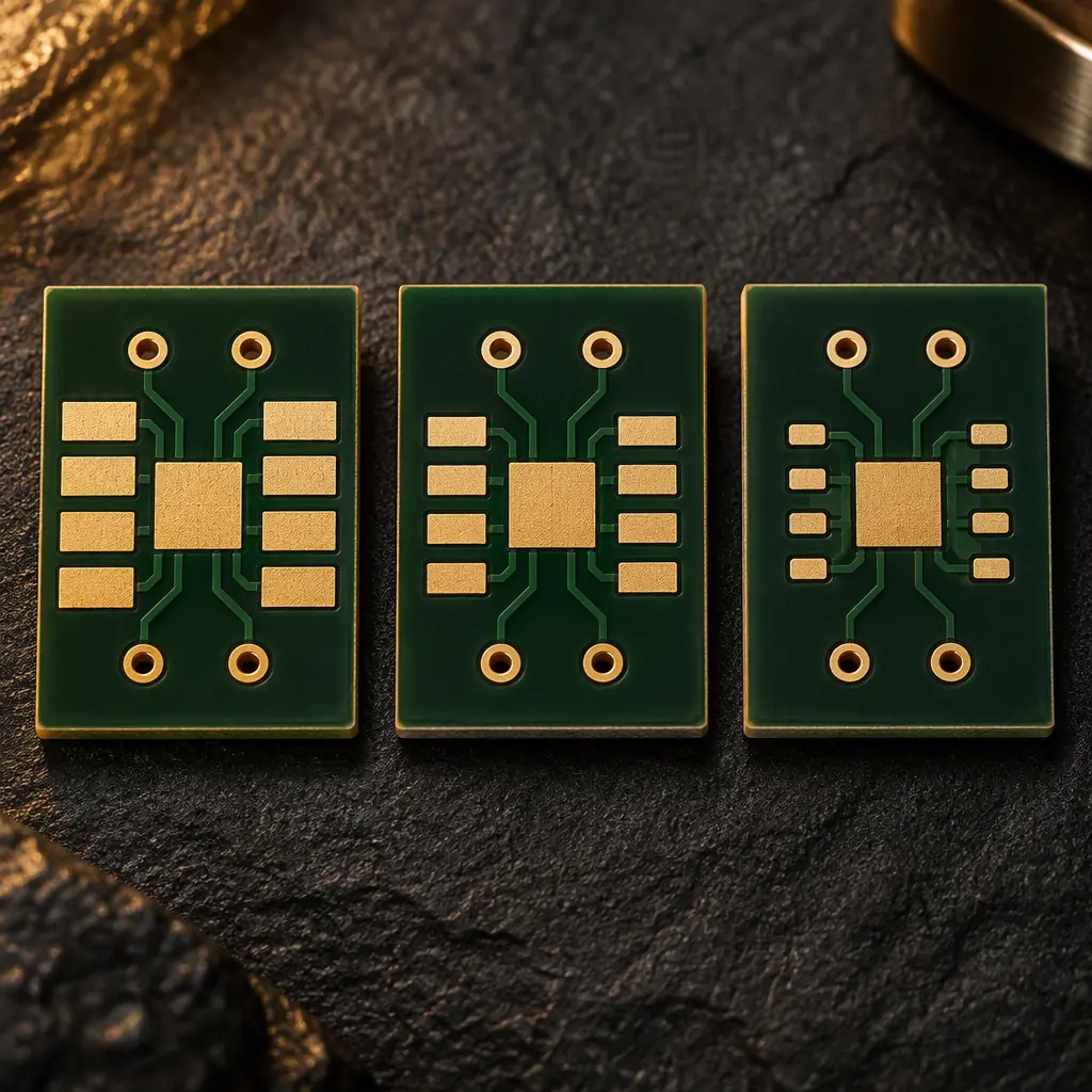
Two engineers can hand you a Gerber set for the identical circuit and get back two boards with completely different solder defect rates. The schematic is the same, the BOM is the same, the fab tolerance is the same. What differs is the land pattern — the copper pad geometry underneath every component. And in the industry standard that governs land patterns, IPC-7351, the same 0402 capacitor is formally entitled to three different pad sizes depending on which density level you declared.
That declaration is usually implicit. Most CAD libraries ship a default footprint library, and whatever density level that library was built to becomes your factory-wide standard by accident. It is one of the cheapest decisions in a PCB program to get right and one of the most expensive to discover late. At Huaxing PCBA we fabricate and assemble across 8 SMT lines with placement down to 0201 metric and 0.35 mm pitch, so we see the consequences of footprint choice in first-pass yield data every week.
What IPC-7351 Actually Standardises
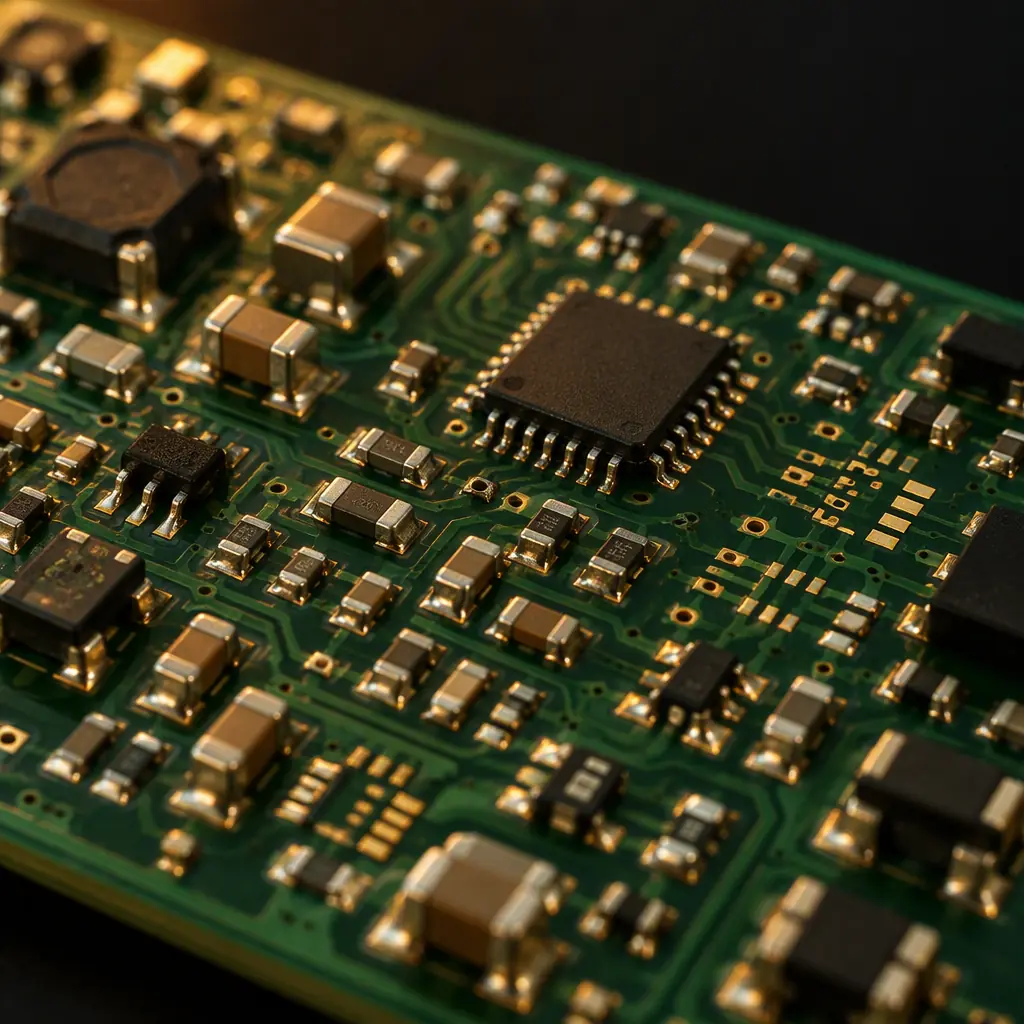
IPC-7351 is the surface-mount design and land pattern standard. Its older revisions were written as prescriptive tables — you looked up your package, you read the pad dimensions off a chart. The modern revision, IPC-7351B, changed the philosophy: instead of fixed tables it defines a calculation method that derives pad geometry from the component's own tolerance band plus the manufacturing process tolerances around it.
That matters commercially, because it means the pad is no longer a fixed property of the component. It is a negotiated outcome between the component datasheet, your placement accuracy, your paste deposition capability and your reflow process window. The standard gives you a formula; your supply chain gives you the inputs.
| Input into the land pattern calculation | Where it comes from | Typical tolerance |
|---|---|---|
| Component terminal tolerance | Datasheet drawing | ±0.05 to ±0.10 mm |
| Placement accuracy | Pick-and-place machine spec | ±0.03 to ±0.05 mm (chip shooter) |
| Solder paste deposition | Stencil aperture fidelity | ±0.025 mm at 0.5 mm pitch |
| Board fabrication tolerance | Fabricator drill/etch capability | ±0.075 mm (standard), ±0.05 mm (fine) |
| Reflow self-alignment | Process window, surface finish | Recovers 0.05 to 0.15 mm of offset |
The output of the calculation is a set of minimum fillet goals: the toe fillet (solder visible beyond the component terminal), the heel fillet (solder behind the terminal toward the body), and the side fillet (solder beside the terminal). These are not cosmetic. Each one maps directly to a defect mode when it is missing.
The Three Density Levels, and What They Cost You
IPC-7351B formalises three density levels. They are not quality tiers — a Level A board is not "worse" than a Level C board. They are trade-offs between solder joint robustness and board real estate, and the standard explicitly ties each to an end-product class.
Maximum (Least) Density — the widest pads, the strongest joints
Fillet goals are generous: the largest toe, heel and side fillets the calculation allows. Pad-to-pad clearance is at its maximum, so stencil apertures can be wide and paste release is forgiving. The cost is board area — a fine-pitch package on Level A can occupy 30 to 50 per cent more footprint area than the same part on Level C. This is the level to choose for military, aerospace, medical implants, automotive underhood and anything that will see thermal cycling, vibration or repeated rework. If a joint will ever be reworked by hand, Level A is the reason it survives.
Nominal (Median) Density — the default for most commercial work
The middle of the calculated tolerance band, with fillet goals sufficient for a well-controlled reflow process but no contingency for a bad process day. This is the correct default for mainstream industrial, telecom, consumer and IoT assemblies where board area matters but the process is stable. If your fab and assembly house are the same supplier and process control is documented, Level B is usually the right economic answer. It is what most professional CAD libraries ship as their nominal footprint set.
Minimum (Most) Density — smallest pads, highest routing value
Smallest permitted pads with the tightest clearance, which frees routing channels and shrinks the board. The fillet goals are the minimum that the calculation permits, which means the process window is narrow — paste volume has to be right on target and placement has to be accurate, because there is no surplus pad area to absorb error. This level is for high-volume, stable, space-constrained consumer products assembled on a mature line: smartphones, wearables, high-density modules. It is a bad choice for low-volume, high-mix or prototype work, and a bad choice for anything that will be reworked.
Key Takeaway: Density level is a process-contingency decision, not a size preference. Level A buys you process margin with board area; Level C buys you board area with process margin. If you cannot state your line's actual placement accuracy and paste Cpk, you do not yet have the data to choose Level C safely — default to Level B and revisit after you have yield data. See our guide to SMT first pass yield diagnosis for how to read those numbers.
Where the Fillet Goals Come From — and What Breaks Without Them
Each fillet has a specific job, and the defect it prevents is well documented in acceptance standards. The table below maps fillet goal to failure mode; this is the reasoning that should sit behind every footprint you approve.
| Fillet goal | What it protects against | Typical consequence when undersized |
|---|---|---|
| Toe fillet (outboard) | Opens (no-contact) joints, weak joint under thermal cycling | Joint passes AOI but fails thermal cycling or drop test |
| Heel fillet (inboard) | Fillete lift, tombstoning on small passives, inadequate joint volume | Tombstoning on 0402/0201; intermittent opens after reflow |
| Side fillet (lateral) | Solder bridging between adjacent pads, misalignment tolerance | Bridging at fine pitch; poor self-alignment during reflow |
| Pad-to-pad clearance | Stencil web collapse, paste smearing, bridging | Solder balls, bridges, chronic shorts at 0.4 mm pitch and below |
The heel fillet is the one buyers most often ignore, and it is the one that ruins small-passive assemblies. On a 0402 or 0201 chip capacitor, the heel fillet provides most of the joint volume and virtually all of the restoring force during reflow self-alignment. Cut it too small in pursuit of density and the part behaves unpredictably: some units align perfectly, others tombstone, and the defect shows up as a yield loss you cannot reproduce on the bench.
The Nominal-vs-Actual Trap in CAD Libraries
Here is the part most procurement and engineering managers do not see. A PCB design tool's bundled library is generated to one density level, usually nominal. When a designer works from that library and the fabrication house applies its own standard shrink or growth to suit its process, the two adjustments can compound.
Our recommendation is procedural rather than technical: state the density level explicitly in the fabrication drawing. A note reading "land patterns per IPC-7351B, Level B, unless otherwise noted" removes the ambiguity entirely. Where specific parts need a different level, say so on the drawing with a part reference. This costs one line of text on a drawing and eliminates a whole class of late-stage disputes about who was responsible for a footprint that was nominally compliant but process-unsuitable.
Assembly drawing and fabrication drawing content is its own subject — our Gerber files guide covers what belongs in the manufacturing data package, and PCB manufacturing tolerances covers the values a fabricator can actually hold.
How Density Level Flows Through to Stencil and Panel
Density level does not stop at the copper layer. It propagates into the stencil aperture, the paste volume target and the panelisation strategy, which is why changing it late is expensive.
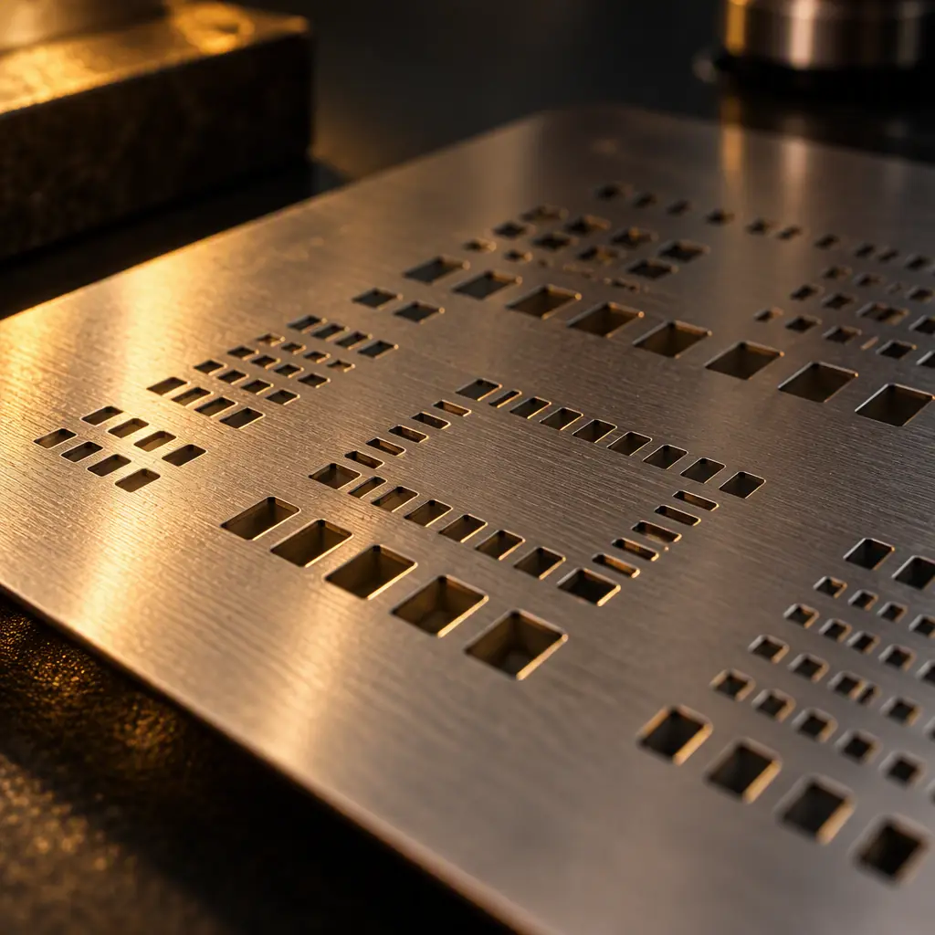
A Level C footprint leaves a narrow web of stencil material between adjacent apertures. At 0.4 mm pitch that web approaches the limit of what laser cutting and stencil tension can hold reliably, and a collapsed web deposits excess paste that bridges. The stencil design therefore has to be tuned in lockstep with the footprint, using aperture area ratios and in some cases home-plate or rounded aperture shapes. Full detail on aperture geometry is in our SMT stencil design guide, and the trade-off between printing and jetting at these geometries is covered in solder paste jetting vs stencil printing.
Paste volume targets move in the same direction. Tighter pads need proportionally tighter volume control, which is a SPI-driven process. Our guide to solder paste volume control with SPI documents the Cpk targets that make a Level C design manufacturable rather than aspirational.
Factory reality check: When a customer sends a Level C footprint set for a 200-piece NPI build, we usually recommend re-authoring to Level B for the prototype stage and reserving Level C for the production release. The copper change is free at Gerber stage and expensive after tooling. The alternative — printing a 0.35 mm pitch Level C layout on a low-volume line — produces first-article yields in the 85 to 92 per cent range where the same layout at Level B typically reaches 97 to 99 per cent.
Choosing a Level: A Practical Decision Path
Strip away the standard's formality and the decision reduces to three questions about the product and three about the process. Answer them in order.
Will this assembly ever be hand-reworked or repaired?
If yes, use Level A. Rework requires a soldering iron tip to reach the joint and a fillet to reflow; a minimum-density pad gives neither. This single question settles the level for most industrial, medical and aerospace control boards, where field repair or depot rework is contractual. Our PCB rework and repair guide covers what a repairable joint actually requires.
What thermal and mechanical environment will the joint see?
Repeated thermal cycling, high vibration or wide operating temperature ranges all consume joint fatigue life, and joint fatigue life scales with fillet volume. Automotive underhood, energy storage, downhole and avionics products belong on Level A regardless of board-area pressure. Our guide to thermal cycling testing shows how the qualification test will expose a marginal joint.
What is the expected volume, and is the process already mature?
Level C is defensible only at high volume on a stable line with documented placement accuracy and paste Cpk. Below roughly 10,000 units a year, or in a high-mix environment where the line changes over frequently, the process contingency that Level C gives away is worth more than the board area it saves. If you are still at prototype stage, see prototype vs mass production for how the process economics shift.
Can you document the process inputs the standard assumes?
The IPC-7351B calculation is only as good as the tolerances fed into it. If your assembler cannot supply placement accuracy, paste deposition capability and reflow profile data, the calculation is running on assumptions. Ask for them — our factory visit checklist lists the process documentation a buyer should request, and the supplier audit guide covers what a credible process-control answer looks like.
Have you checked the level on your existing library?
Before writing any new footprints, establish what your current library already contains. If it is a nominal set, note that explicitly in the drawing package. Mixing levels within one library without documentation is a common and avoidable source of footprint disputes, and it complicates DFM review because the fabricator cannot tell which pads are intentional. Our DFM tips and shift-left DFM verification guides cover how to surface these issues before tooling.
Summary and Next Steps
IPC-7351 density level is a documented trade-off between solder joint robustness and board area, and it belongs in the fabrication drawing where everyone can see it. Level A buys process margin, Level C buys space, Level B is the commercial default. Choose it deliberately, document it explicitly, and revisit it once you have real yield data from your line.
At Huaxing PCBA we review land patterns at DFM stage rather than after tooling, because a pad change at Gerber stage is free. Our engineering team holds IATF 16949 and ISO 9001 certification and runs SMT placement to 0.35 mm pitch with SPI-verified paste deposition across 8 lines. Read our stencil design guide or send your Gerber files for a free DFM review with your quote, returned within 24 hours.
