
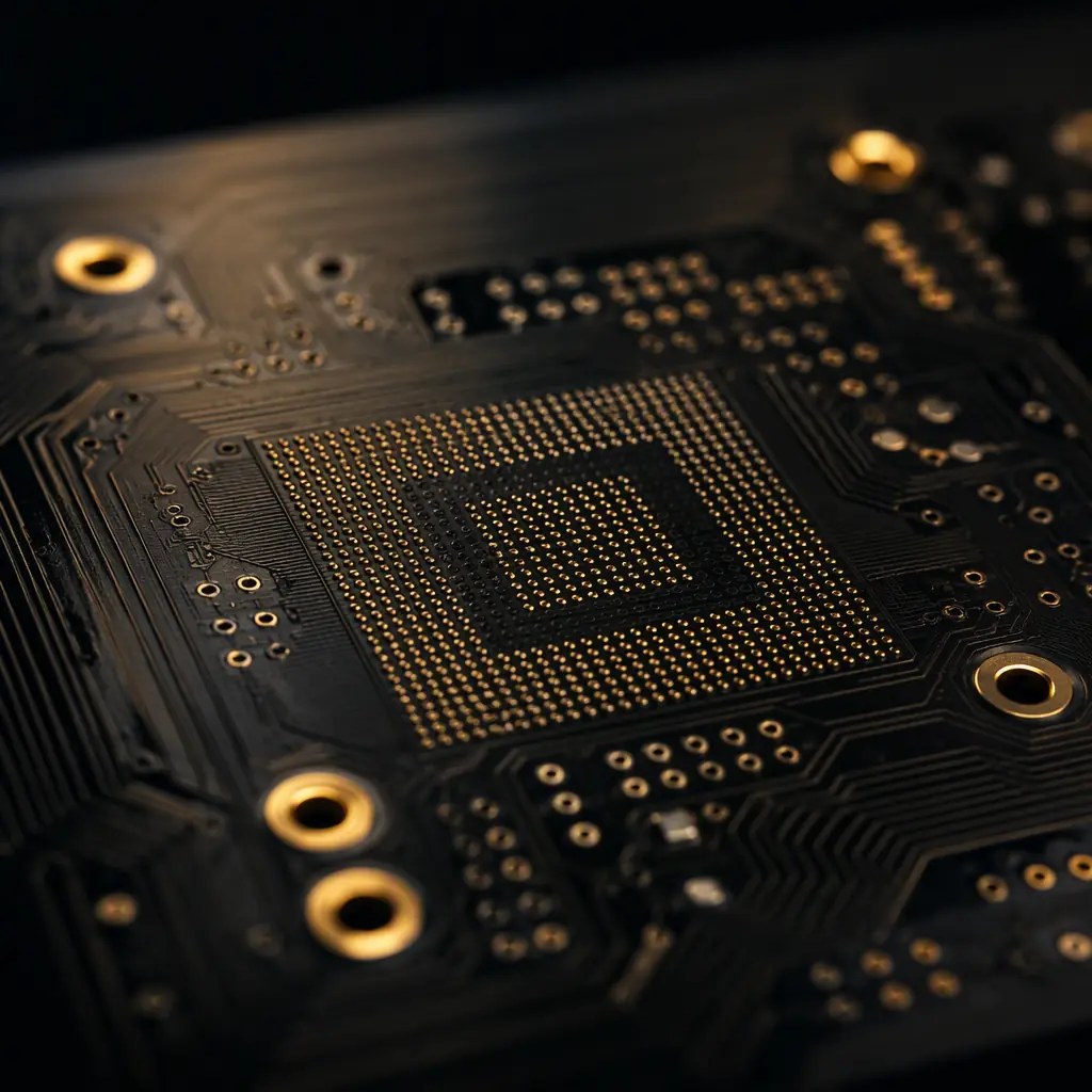
A filled via is a plated through-hole or microvia whose cavity is plugged with a material, copper, resin, or conductive paste, after plating. On the fabrication drawing it is one line: "filled vias, IPC-4761 Type VII." In the factory it is an entire process sequence that changes your cost per hole by 2–6x, and in the field it is often the difference between a board that survives 10 years of thermal cycling and one that fails at the solder joint after 18 months.
Most procurement engineers first meet filled vias when a CM rejects their via-in-pad design or quotes a surprise premium. Huaxing PCBA produces 8,000+ filled-via board designs per year across automotive, medical and telecom programs, and this guide walks through the decision from the drawing side: what the IPC-4761 types mean, when each is mandatory, and what you actually pay.
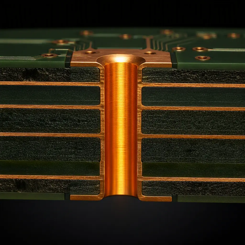
What IPC-4761 Actually Defines: Seven Via Protection Types
IPC-4761 is the industry standard for via protection. It defines seven types, and understanding them prevents the most common spec error: writing "tented vias" when you need a filled via, or paying for copper fill when resin fill would do. The seven types are organized into three families, cap, tent, and fill:
| IPC-4761 Type | Method | Typical Use | Relative Cost |
|---|---|---|---|
| Type I | Tented with dry film / solder mask | Cheap, non-critical inner layers | Baseline |
| Type II | Tented and covered (solder mask over cap) | Outer layers, low-density designs | +10% |
| Type III | Plugged with non-conductive material | Via-in-pad with mask-defined openings | +40% |
| Type IV | Plugged and capped (mask over plug) | Via-in-pad, soldered surface | +50% |
| Type V | Filled with conductive paste | Via-in-pad, solderable fill | +60% |
| Type VI | Filled with conductive paste and capped | Via-in-pad, best solderability | +70% |
| Type VII | Filled with plated copper | HDI microvias, high-current, thermal vias | +100%+ |
The distinction between "plugged" (Types III–IV) and "filled" (Types V–VII) matters: plugged vias are sealed against solder wicking, filled vias provide a solid, flat, electrically usable surface. If your BGA pad design places vias directly in pads, the solderable fill types (V–VII) are the ones that survive reflow without voiding.
Key Takeaway: "Filled via" is not one process. Type IV (plug + cap) is the minimum for via-in-pad with mask-defined openings; Type VII (copper fill) is what HDI microvias and high-current designs actually need. Spec the IPC-4761 type by name on your drawing. "filled via" alone leaves the factory to choose, and the choice affects both cost and reliability.
Via-in-Pad: Why the Fill Type Is Non-Negotiable
Via-in-pad, placing a via inside an SMT pad, is the standard escape strategy for fine-pitch BGAs below 0.8 mm pitch. At 0.4–0.5 mm pitch, routing channels between pads disappear and vias must go inside the pads. But an unfilled via in a pad has three failure modes: solder wicking down the barrel (starving the joint), outgassing voids during reflow, and poor flatness that breaks the solder paste print.
Solder wicking steals joint volume
In reflow, molten solder wicks into an open via barrel by capillary action. On a 0.5 mm BGA pad with a 0.2 mm via, wicking can pull 30–50% of the joint's solder away, producing a head-in-pillow or insufficient solder joint that passes AOI but fails in thermal cycling. Filled vias eliminate the capillary path entirely.
Outgassing voids come from trapped chemistry
Plating chemistry and moisture trapped in an open via barrel vaporize at reflow temperatures. The gas expands during the liquid phase of solder, creating voids that X-ray inspection routinely finds at 5–20% of joint area. IPC-A-610 Class 3 allows limited voiding, but voids above 25% of the joint are field failures waiting to happen, see our BGA assembly guide for the inspection side of this problem.
Surface flatness breaks the stencil print
An unfilled via creates a concave pocket in the pad. The solder paste deposits unevenly, and after reflow you get inconsistent joint heights across the BGA field. Filled and capped vias give a flat, coplanar surface, a requirement for the paste printing process to produce uniform deposits.
Procurement Tip: If your design uses via-in-pad and your drawing does not specify a fill type, ask your CM which IPC-4761 type they will run. A vendor that defaults to Type IV where Type V was needed is a reliability risk hiding in the quote.
Copper-Filled vs Resin-Filled vs Conductive Paste: The Real Difference
Once you know you need a fill, the choice between the three fill materials comes down to three questions: does the via carry current, does it need to conduct heat, and does it sit in a soldered pad?
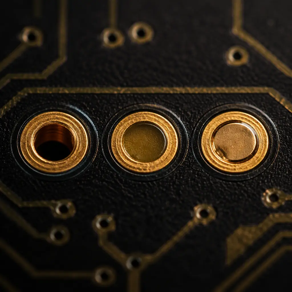
Copper-filled vias (Type VII)
Copper fill is performed by electroplating. The via is filled with plated copper in a controlled plating cycle, then planarized. The result is a solid copper plug with the same conductivity as the surrounding copper. This is the required solution for:
- HDI microvias in stacked configurations, where the microvia becomes a structural part of the interconnect
- Via-in-pad on high-current power planes, where the via itself is part of the current path
- Thermal vias under power components, where copper's thermal conductivity (~385 W/m·K) matters
- Any via that will later be stacked with another via above it
Copper fill costs the most, roughly 2–3x the per-hole cost of resin fill, because it adds an electroplating step with tight process control. If you do not need the electrical or thermal conduction, you are paying for capability you will not use.
Resin-filled vias (Types III–IV)
Resin (epoxy) fill is the workhorse of via-in-pad. A non-conductive plug seals the via, and the cap provides a flat, solderable surface. Resin fill does not carry current, but the surrounding barrel plating does, the fill only blocks the cavity. This covers the majority of fine-pitch BGA escape routing where the via connects a signal layer to an inner layer and current density is low. It is the most common spec on smartphone-class boards and is fully adequate for most digital designs.
Conductive paste fill (Types V–VI)
Conductive paste fill sits between the two: it provides a solderable plug and some electrical continuity, at lower cost than plated copper. It is used where via-in-pad must be solderable but current requirements are modest. Paste fill is more sensitive to process variation than copper fill. Porosity in the paste plug can affect long-term reliability, so it is specified less often than either copper or resin in automotive and medical programs.
| Fill Type | IPC-4761 | Current Path? | Thermal Path? | Solderable? | Typical Cost/Hole |
|---|---|---|---|---|---|
| Resin plug + cap | Type IV | No (barrel only) | Poor | Yes (cap) | $0.02–0.04 |
| Conductive paste | Type V/VI | Partial | Moderate | Yes | $0.03–0.06 |
| Plated copper | Type VII | Full | Excellent | Yes | $0.05–0.12 |
HDI Microvias: Where Copper Fill Becomes Mandatory
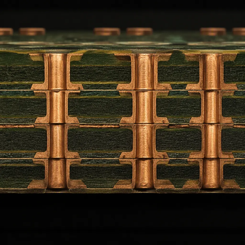
In HDI boards, microvias (≤0.15 mm, laser-drilled) are frequently stacked, via-over-via, to route high-density interconnect across multiple layers. A stacked microvia structure transfers mechanical and thermal stress through the via column, and an unfilled or resin-filled column can crack or delaminate under thermal cycling. Copper-filled microvias form a solid column that passes IPC-6012 qualification and IST (Interconnect Stress Test) requirements.
Our HDI technology guide covers when stacked vs staggered microvias make sense; the manufacturing side is that copper fill is what makes stacking physically reliable. Staggered (offset) microvias can often use resin fill because the stress path does not align vertically, a cost saving worth discussing with your CM before you commit the stackup.
How Filled Vias Change Cost, Real Numbers
Cost impact is the question every procurement engineer asks, and the honest answer is: it depends entirely on via count and fill type. On a typical 8-layer board with 2,000 vias, moving from tented (Type I) to resin plug + cap (Type IV) adds roughly $0.03–0.05 per board in direct cost, small on an expensive BGA assembly, significant on a high-volume consumer board. Moving 400 of those vias to copper fill for HDI sections adds another $0.03–0.06.
Count your true via-in-pad population
Only the vias inside pads need fill. Vias in the BGA field but outside pads can be tented or plugged at lower cost. A proper DFM review separates these populations before quoting, see our DFM checklist for the review process.
Segregate fill types by zone
A well-optimized board uses copper fill only where needed (stacked microvias, power vias) and resin fill elsewhere. Specifying one fill type for the entire board is simpler but costs more than necessary.
Ask for the fill in the drill chart
Put fill requirements in the fabrication drawing drill table, not buried in general notes. "All vias in BGA pads: IPC-4761 Type IV; microvias 0.10 mm: Type VII" is unambiguous and quotable.
Cost Reality: Filled vias are not a luxury spec. On fine-pitch BGA boards they are the difference between a functional product and a field-failure rate that kills the program. The $0.03–0.05 per board is insurance against rework costs measured in hundreds of dollars per failed assembly.
DFM Rules for Filled Via Designs
Before you send the files, run these checks. They are the top five rejection reasons our engineering team sees on filled-via designs:
Via diameter vs fill capability
Copper fill is practical for microvias up to about 0.25 mm. Above that, plating a solid copper plug takes long cycle times and becomes uneconomical, switch to resin fill or via-in-pad with plug + cap.
Aspect ratio limits
Fill processes have aspect-ratio limits. Resin fill handles aspect ratios up to about 10:1 for typical production; copper fill is most reliable below 4:1. Deep, narrow vias may require process consultation before the quote.
Planarization and surface finish interaction
After copper fill, the surface is planarized (typically by belt sanding or chemical mechanical polishing). This exposes fresh copper that then receives the surface finish, ENIG or ENEPIG are common on filled-via boards. Make sure the finish is specified over the filled vias; our surface finish guide covers the options.
Inspection requirement
Filled vias are verified by cross-sectioning, the microsection report shows fill integrity, cap thickness and voiding. Specify microsection sampling on the drawing (typically 2–3 coupons per panel) and request the report with first articles. Our microsection analysis guide explains how to read the report.
Thermal reliability qualification
For automotive and medical programs, filled-via boards should be qualified with thermal cycling per IPC-9701: typically 500–1000 cycles from -40°C to +125°C. Copper-filled vias pass; poorly controlled resin fill can crack at the plug/barrel interface. Our thermal cycling guide details the test matrix.
Summary: Spec the Type, Not the Word
The single most important habit for filled vias is precision in the specification. Write the IPC-4761 type on the drawing, count the via-in-pad population accurately, segregate fill types by zone, and verify with microsection on first articles. Copper fill for HDI stacks and current-carrying vias; resin plug + cap for the rest; conductive paste only where solderable fill is needed at moderate cost.
At Huaxing PCBA, our production lines process copper-filled microvias down to 0.075 mm laser-drilled diameters with any-layer HDI stacking up to 32 layers. Every filled-via order ships with microsection verification on request, and our engineering team reviews your via strategy during the free DFM check. Read our via technology guide for the wider via-selection framework, or contact our engineering team with your stackup for a project-specific fill recommendation.
