
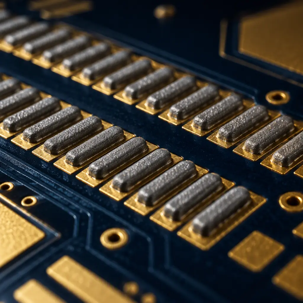
Most solder defects on a finished board are printing defects that were decided weeks earlier, in the seconds it took a squeegee to cross a stencil. Insufficient paste becomes an open joint. A slumped deposit becomes a bridge. A bead of paste under the stencil becomes a loose solder ball rolling around inside the enclosure. By the time reflow is finished, the print process is already out of reach.
This guide covers the eight printing defects worth knowing, in each case pairing the visual symptom with the print parameter that causes it and the correction that reliably holds in production. It deliberately stays on the printer and stencil side; where a defect is really a stencil-design problem rather than a printer-setting problem, the link points to the page that covers that layer properly.
The Print Window — Where These Defects Are Born
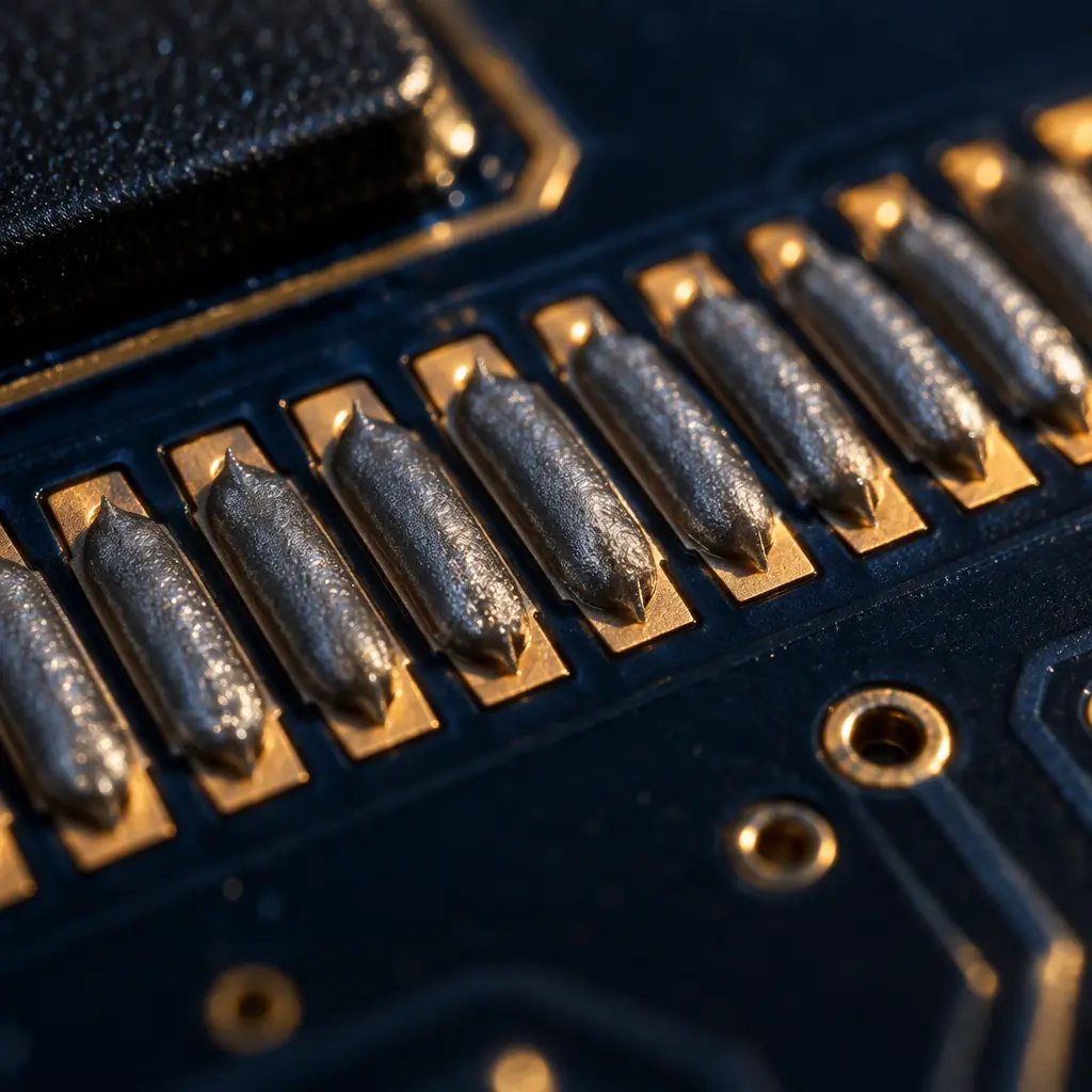
Every paste deposit is the result of four variables that have to be balanced: stencil aperture geometry, paste rheology, squeegee pressure and speed, and the separation speed at which the board drops away from the stencil. Get the balance right and deposits are uniform across the panel. Get it wrong and you get one of the defect signatures below, often on only part of the board.
Three parameter ranges matter for most corrections. Squeegee durometer typically sits between 80 and 90 Shore A, with softer blades conforming better to uneven surfaces and harder blades holding aperture definition on fine pitch. Print speed is generally in the 20 to 80 mm/s range, with faster speeds producing better paste release on fine features but a higher risk of insufficient fill on coarse ones. Separation speed is much slower than print speed, commonly 2 to 5 mm/s, and it is the single most under-adjusted parameter in facilities that are chasing insufficient-paste defects.
Key Takeaway: Before changing paste or alloy, change separation speed. It costs nothing, it is a one-line recipe edit, and it resolves a large share of insufficient-paste and torn-deposit defects that get mistakenly attributed to the material.
| Parameter | Typical Range | Effect of Increasing |
|---|---|---|
| Squeegee durometer | 80-90 Shore A | Better aperture definition, worse conformity to uneven panels |
| Print speed | 20-80 mm/s | Improved release on fine pitch, worse fill on coarse features |
| Squeegee pressure | Typical start 1 kg per 25 mm of blade | Cleaner wipe, higher stencil wear and aperture wear |
| Separation speed | 2-5 mm/s | Cleaner release, longer cycle time |
Insufficient Paste and Skipped Deposits
Insufficient paste is a deposit that is present but under volume; a skipped deposit is absent entirely. Both produce open joints after reflow, and both are volume failures rather than chemistry failures.
Symptom and Why It Matters
The deposit is visible but shallow, or the pad is bare. After reflow the result is a weak fillet at best and an open joint at worst, and the failure can be intermittent — a joint that forms but is thin may pass functional test and fail in the field under thermal cycling. This is the defect class that most often escapes into shipped product.
Cause: Separation Speed and Aperture Aspect Ratio
Paste adheres to both the pad and the aperture wall. If the board drops away faster than the paste can release, part of the deposit stays in the aperture. The problem compounds as aperture area shrinks: a small, deep aperture has a high wall area relative to its volume, so adhesion to the wall dominates. This is where stencil design and printer settings meet, and aperture geometry itself is covered in our guide to SMT stencil design.
Fix: Slow the Separation, Then Check the Aperture
Reduce separation speed toward the low end of the range, then re-measure with SPI. If the deposit improves but is still low, the aperture is the constraint and needs area-ratio attention rather than more printer tuning. Stencils also wear: tension loss and aperture wall build-up both degrade release over a stencil's life, which is why stencil lifecycle management belongs in the same conversation as printer settings.
Bridging and Slumping
Bridging is paste joining two adjacent pads before component placement. Slumping is the related failure where a deposit holds its shape on the stencil but flows sideways after separation, with the bridge forming later. Both end as solder bridges after reflow.
Symptom
A visible paste connection between adjacent pads immediately after print (bridging) or a deposit whose footprint has spread beyond the pad edge by the time the SPI camera sees it (slumping). On fine-pitch devices the two are visually similar at the 0.4 mm and below pitches that make the defect dangerous.
Cause: Excess Volume, Low Viscosity, Contamination
Bridging on the print occurs when too much paste is deposited and squeezed sideways under the squeegee, typically from excessive pressure or an oversized aperture. Slumping indicates the paste has lost viscosity — usually because it has been open too long, has been reworked, or has absorbed moisture. Paste that is outside its handling window behaves differently in exactly this way, and the storage rules are set out in our guide to solder paste storage and handling to J-STD-005.
Fix: Confirm the Paste First, Then the Pressure
Slumping with an otherwise stable process is a paste-freshness signal: verify open time and check whether the lot is within its handling window before adjusting the printer. Where bridging is a pure volume failure, reduce squeegee pressure and verify aperture sizing. Alloy and flux selection also affect slumping tendency, which is covered in our solder paste selection guide.
Solder Beading and Mid-Chip Beads
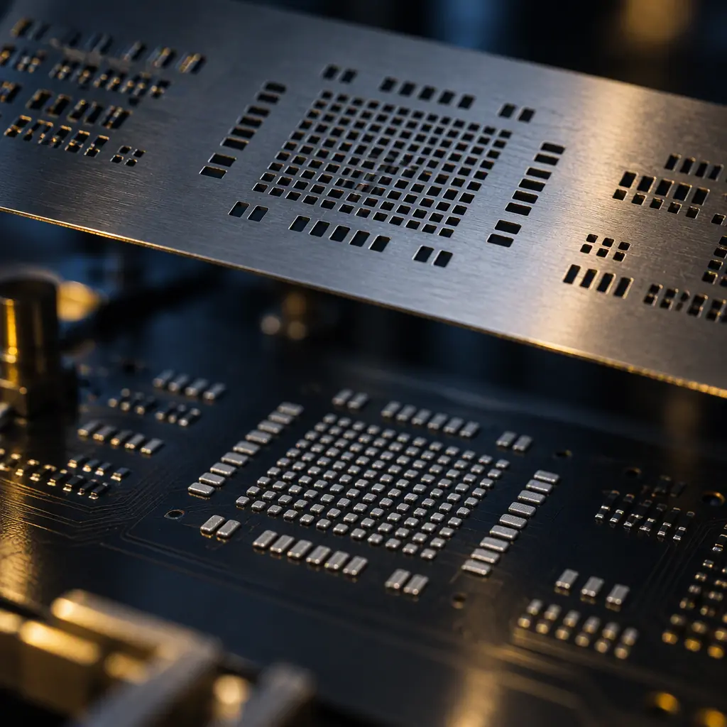
This is the defect that most generic printing-defect lists omit, and it is the one that creates the worst customer experience — a loose solder ball found inside a sealed enclosure during final inspection or, worse, after shipping.
Symptom
Small, spherical solder balls sitting adjacent to a chip component or scattered on the board surface after reflow. Mid-chip beads specifically form on the sides of chip resistors and capacitors, between the two terminations.
Cause: Paste Squeezed Under the Stencil
The dominant mechanism is paste forced beneath the stencil onto the board surface — through a poor stencil-to-pad seal, a warped or under-tensioned stencil, or excessive squeegee pressure driving paste sideways under the aperture wall. Solder mask between the pads (the mid-chip area) then traps it, and reflow turns the trapped paste into a bead. Another contributor is paste on the underside of the stencil transferring to the board, which becomes more likely as a stencil accumulates prints without cleaning.
Fix: Seal, Tension and Cleaning Frequency
Verify stencil tension is within specification, reduce squeegee pressure, confirm the board support is flat and adequate, and increase the cleaning frequency on the underside of the stencil. Because the primary driver is stencil condition, this defect is addressed jointly with the practices in our stencil lifecycle guide.
Dog-Earing, Torn Deposits and Stencil Clogging
These three are grouped because they share a mechanical cause: paste failing to release cleanly from the aperture wall.
Dog-Earing
The deposit is rounded or peeled up at one corner, resembling a dog's ear. It occurs when release is uneven across an aperture, usually the result of aperture wall roughness, insufficient separation dwell, or paste drying at the edges of the aperture. Left uncorrected it produces skewed component placement and a weak joint on the affected corner.
Torn Deposits
Part of the deposit stays in the aperture while the rest transfers, leaving a deposit with a visibly ragged top surface and reduced volume. The cause is the same adhesion-versus-release balance as insufficient paste, but with the failure occurring mid-deposit rather than across the whole aperture. Reducing separation speed is the first correction.
Stencil Clogging
Paste dries in the aperture during the run and progressively blocks it, so deposit volume declines across the shift. The signature is a gradual downward drift in SPI volumes rather than a step change, and it is the reason SPI trend data is more useful than a single snapshot. Cleaning interval, paste open time and ambient humidity all drive the rate.
Defect → Parameter → Fix
Use this as the first-response table when a printing defect appears on the line. It maps what the operator sees to the parameter most likely responsible and the first change to make.
| Defect | Symptom Signature | Most Likely Parameter | First Correction |
|---|---|---|---|
| Insufficient paste | Shallow deposit, low SPI volume | Separation speed too high; aperture area ratio | Reduce separation speed; review aperture geometry |
| Skipped deposit | Bare pad, zero volume | Clogged aperture; stencil seal | Clean stencil; inspect aperture condition |
| Bridging | Paste joining adjacent pads at print | Squeegee pressure; aperture oversized | Reduce pressure; verify aperture size |
| Slumping | Deposit spreads after separation | Paste viscosity, open time exceeded | Verify paste handling window and lot age |
| Solder beading | Loose balls beside chip parts | Stencil seal, tension, underside cleanliness | Check tension; reduce pressure; clean more often |
| Mid-chip beads | Balls in the mask between terminations | Paste squeeze-out under stencil | Improve board support and stencil seal |
| Dog-earing | Deposit rounded or lifted at one corner | Aperture wall condition; dwell time | Inspect aperture walls; increase separation dwell |
| Torn deposit | Ragged top surface, reduced volume | Separation speed | Reduce separation speed incrementally |
| Clogging | Volume drifts down across the shift | Cleaning interval; paste open time | Reduce cleaning interval; control humidity |
Whichever defect you are chasing, the confirming measurement is the same: SPI volume data per aperture, trended rather than spot-checked. The Cpk targets and process windows worth holding are set out in our guide to solder paste volume control with SPI. Where the correction touches a leadless package with an exposed pad, the aperture and coverage requirements are different again, as covered in our article on QFN and LGA leadless package soldering.
Summary
All eight defects reduce to the balance between paste adhesion and paste release, modulated by how well the stencil seals against the board. Separation speed, squeegee pressure and stencil condition account for the majority of production printing defects, and all three are adjustable without changing material or design. Where a defect resists printer tuning, the constraint is usually aperture geometry, which is a design fix rather than a process fix.
Because these defects are decided before reflow, detection has to happen before reflow. That means SPI on every board and a supplier who can show you volume Cpk data rather than a visual inspection pass. The inspection sampling that supports that claim is covered in our AQL sampling guide.
At Huaxing PCBA, our SMT lines run SPI on every print with 100 percent volume data capture, and our process engineers hold board-specific print recipes rather than a single line default. We review aperture area ratios at DFM stage so that fine-pitch features are printable before tooling is cut. Read our stencil design guide or contact our engineering team to review your assembly's printability.
