
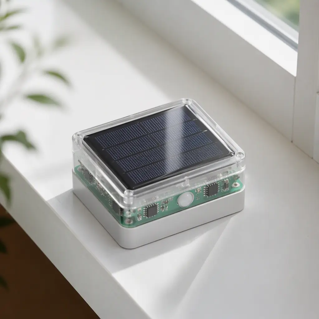
Battery-powered IoT nodes carry a hidden tax: every device with a battery needs a service visit eventually, and at 1 million deployed sensors, that tax becomes a full-time logistics operation. Energy harvesting removes the battery from the equation, the device draws its operating power from ambient light, vibration, heat, or radio waves. The engineering challenge moves from "how much battery do we need" to "how do we make every microwatt count."
This guide covers the PCB-level decisions that separate harvesting designs that work in the field from lab demos that die in a drawer: realistic power budgets per energy source, cold-start power management IC selection, storage architectures, leakage control, and the assembly quality rules that matter at nanoamp currents. We fabricate and assemble these low-power boards at Huaxing PCBA: including the clean-assembly processes leakage control demands. For the connectivity side of a battery-free node, pair this with our IoT PCB design guide.
Power Budget Reality: What Each Energy Source Actually Delivers
The first rule of harvesting design: never size a system from datasheet maximums. Use the realistic range for the deployment environment, and design the power budget around the worst month, not the best day.
| Energy Source | Realistic Power Density | Typical Duty Cycle Supported | Best Deployment |
|---|---|---|---|
| Indoor photovoltaic (office light) | 10-100 µW/cm² | Sensor read every 1-15 min | Smart buildings, retail tags |
| Outdoor photovoltaic | 10-15 mW/cm² | Continuous + wireless uplink | Agriculture, infrastructure |
| Thermoelectric (ΔT 5-10°C) | 10-100 µW/cm² | Sensor read every 5-30 min | Industrial pipes, HVAC, wearables |
| Piezoelectric vibration | 1-100 µW/cm³ | Burst mode, event-driven | Machinery, bridges, vehicles |
| Ambient RF (Wi-Fi/cellular) | 0.1-10 µW/cm² | Sensor read every 30-120 min | Urban sensing, warehouses |
| Dedicated RF (reader-powered) | 10-100 µW/cm² | On-demand activation | RFID, industrial tracking |
Know your sensor's real energy per reading
A typical low-power MCU sleep current is 1-3 µA; waking, reading a sensor, and transmitting one LoRaWAN packet costs roughly 50-150 mJ of energy over 100-300 ms. At 50 µW average harvested power, that is one reading every 15-60 minutes. Design the duty cycle around this arithmetic, not around the datasheet's "ultra-low-power" marketing language. LoRaWAN uplink budgets are detailed in our LoRaWAN and Sub-GHz design guide.
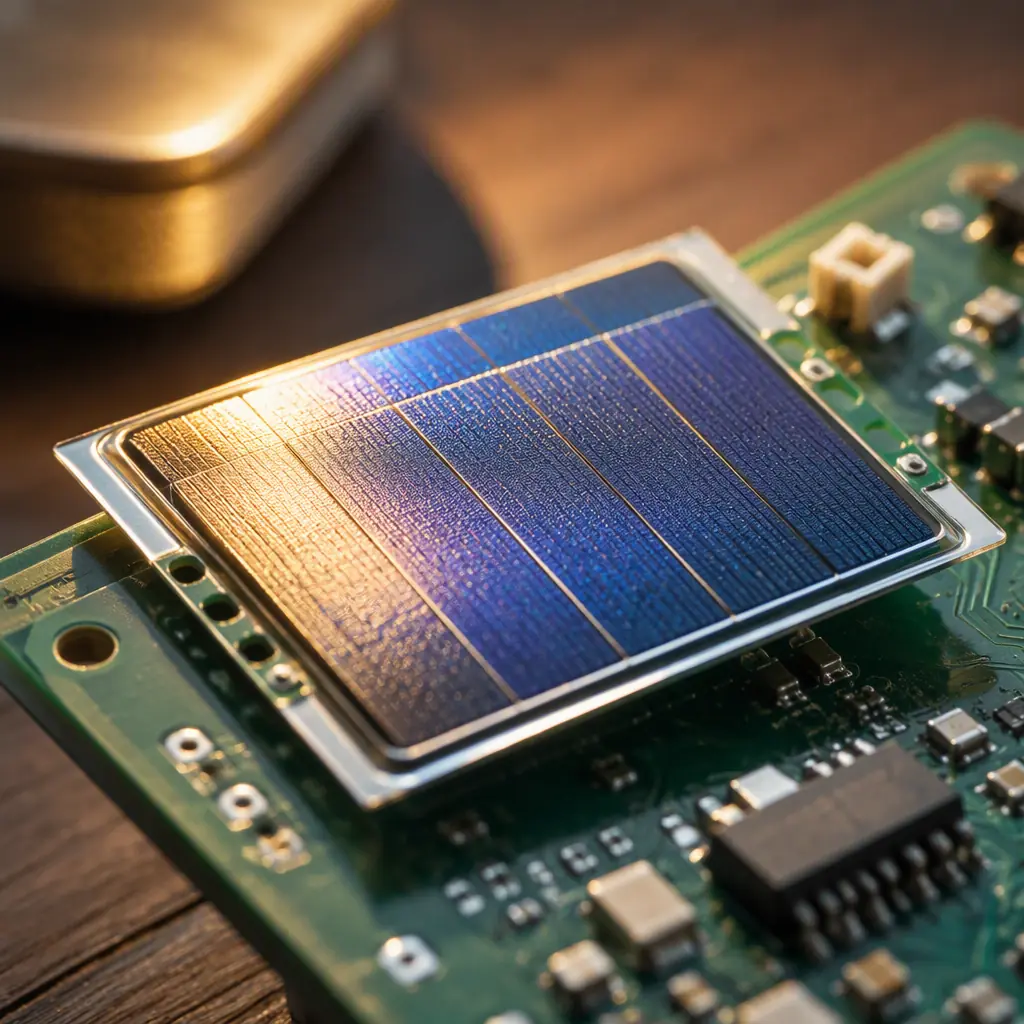
Indoor solar is the workhorse of battery-free IoT
Amorphous or dye-sensitized cells deliver 10-100 µW/cm² under typical 200-500 lux office lighting. A 5 cm² panel in a well-lit office provides 0.5-2 mW, enough for frequent sensing. The design implication: the PCB must reserve a large, flat, uncluttered panel area, because panel size is the single biggest lever on your power budget.
Vibration and RF are event harvesters, not continuous supplies
Piezoelectric harvesters excel where vibration is constant (pumps, compressors) but deliver bursts, not steady power. RF harvesting is viable only where a strong source exists (dedicated readers, dense cellular). Design these as "top-up" sources paired with storage, not as the primary energy budget. For RF-coupled power specifically, our wireless power transfer guide covers the coil and matching network design.
Cold-Start Power Management: The IC That Makes It Possible
Harvesting PMICs do three jobs: boost the low source voltage, manage energy storage, and cold-start from a completely dead state. The cold-start spec is the one most designs get wrong.
Cold-start voltage decides your minimum light level
Modern harvesting PMICs cold-start from 330-600 mV input, some below 100 mV with an external charge pump, and then run with quiescent currents of 300 nA to 1 µA. If your panel delivers 0.5 V under dim light and the PMIC needs 600 mV to start, the device never wakes. Match the PMIC's cold-start threshold to the source voltage at your worst-case lighting, not typical lighting.
MPPT is not optional for solar harvesting
Maximum power point tracking squeezes 20-40% more energy from a solar cell under varying light. Harvesting PMICs with built-in MPPT (typical tracking efficiency 80-90%) pay for themselves in panel area reduction. For thermoelectric sources, the PMIC must handle both polarities, the temperature gradient reverses when a pipe cools below ambient.
Quiescent current is a spec you hold the PMIC to
Every nanoamp of PMIC quiescent current competes with your sensor budget. At 300 nA and 3.3 V, a PMIC consumes 1 µW, acceptable against a 50 µW harvest. At 5 µA quiescent, the PMIC alone eats 16 µW, and your duty cycle collapses. Read the quiescent figure at the actual operating voltage, not the minimum in the datasheet. Power integrity design for these rails is covered in our PDN design guide.
Key Takeaway: Size the harvester for the worst month, pick the PMIC by cold-start voltage and quiescent current at your operating point, and let MPPT do the panel optimization. This combination is what separates field-deployable nodes from demo boards.
Storage Architecture: Supercapacitors vs Thin-Film Batteries
Harvested energy is bursty; the load needs steady power. The storage element bridges the gap, and its chemistry drives board layout and lifetime.
Supercapacitors: the default for battery-free design
Supercapacitors (1-100 F) survive 500,000+ charge cycles, operate from -40°C to +70°C, and contain no lithium, simplifying shipping and disposal. A 10 F cell at 3.3 V holds roughly 54 J, enough for dozens of sensor reads. The layout cost: supercaps are physically large, and their ESR affects inrush current when the radio transmits.
Thin-film solid-state batteries for higher energy density
Solid-state thin-film cells (e.g., 40-100 µAh/mm²-class products) offer 10-20× the energy density of supercaps in a flat, reflow-tolerant package, at higher cost and with a finite cycle life (typically 10,000 cycles or 5-10 years). Use them when the node must survive multi-day dark periods. Their low internal resistance also handles radio burst currents cleanly.
Hybrid: small supercap for bursts, harvester for everything else
Most field nodes end up with a small supercap (1-5 F) as the energy buffer and no battery at all. The design rule: size storage for the worst-case duty period (e.g., 3 days of darkness indoors), then verify the harvester can refill it within the best-case period. Storage sizing methodology is covered in our portable power station architecture guide.
Leakage Control: Why Nanoamps Slip Away on the PCB Itself
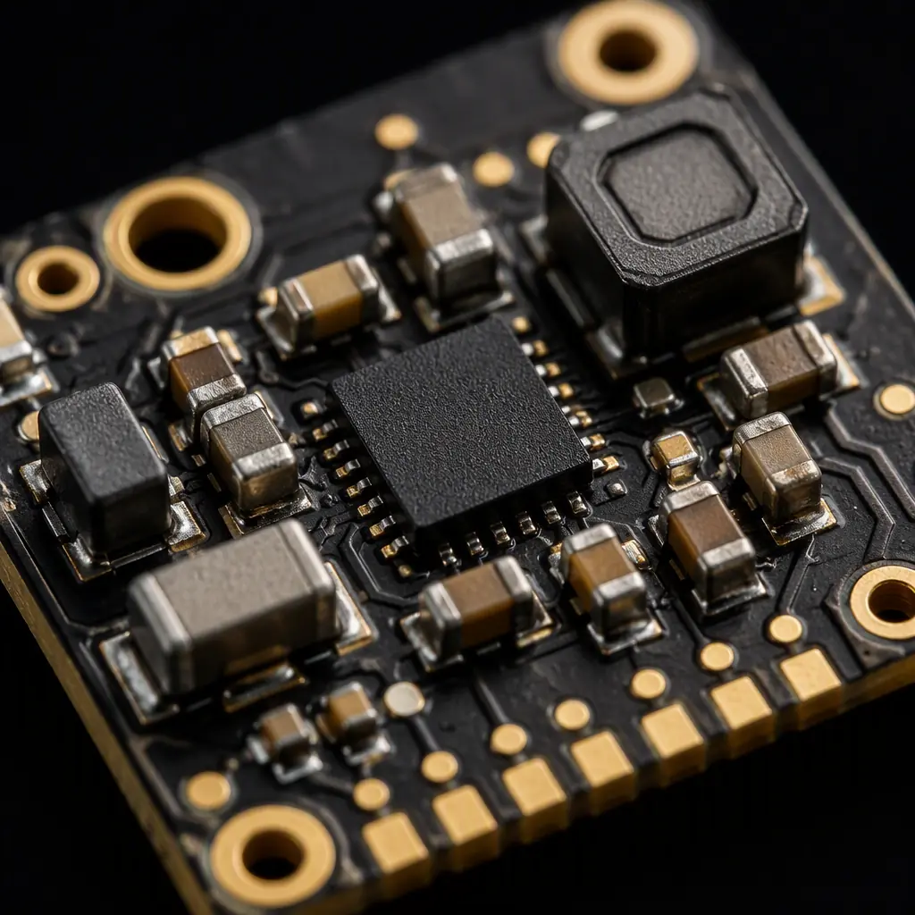
At microamp system currents, the PCB is no longer an ideal insulator. Surface leakage across the board can exceed the entire sensor budget if the design and assembly are not controlled.
Ionic contamination is the #1 leakage source
Flux residue and other ionic contamination on the board surface creates leakage paths that grow with humidity. 100 MΩ between traces at 30% RH can drop below 10 MΩ at 80% RH. For harvesting circuits operating at nanoamp levels, specify aqueous cleaning after soldering and verify with ionic cleanliness testing. Our ionic contamination testing guide explains ROSE and SIR methods, and aqueous vs solvent cleaning covers process selection.
Guard rings and high-impedance node protection
Surround high-impedance sense nodes (photodiode amplifiers, voltage references) with guard rings driven at the same potential, and route them on dedicated clean layers. A 1 cm trace pair with 0.3 mm spacing in clean, dry conditions leaks ~1 pA; the same pair with contamination leaks 1000× more. The analog layout discipline is detailed in our mixed-signal design guide.
Conformal coating for humid deployments
A thin acrylic or Parylene coating eliminates surface leakage in high-humidity environments (agriculture, marine, cold chain): often the difference between a node that sleeps at 1 µA and one that drains at 20 µA in a humid season. Material selection guidance is in our conformal coating guide. For sealed outdoor nodes, moisture sensitivity handling during assembly matters too, see our MSL handling guide.
Antenna and RF Harvesting Front-End Design
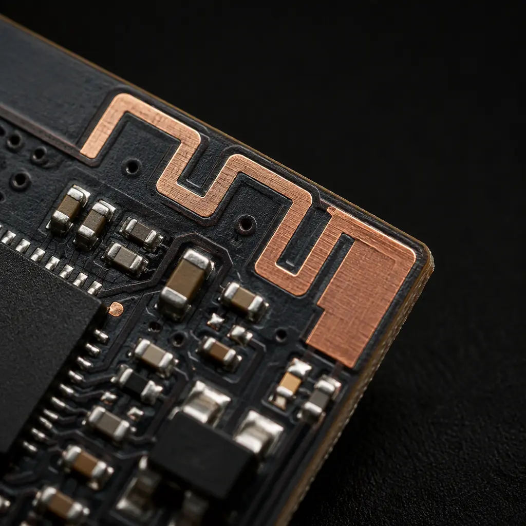
If your node harvests RF or uses a low-power radio, the antenna front-end deserves the same attention as the power path. A 1 dB mismatch costs 20% of your already-tiny energy budget.
Matching network efficiency beats antenna gain at close range
For RF harvesting at 868/915 MHz or 2.4 GHz, a well-matched PCB antenna with a tuned matching network captures more energy than a slightly larger antenna with poor match. Measure return loss at the actual deployment frequency and environment, nearby metal shifts resonance by tens of MHz. Antenna layout and tuning fundamentals are in our PCB antenna design guide.
Keep the harvesting rectifier close to the antenna
The RF-to-DC rectifier (often a voltage multiplier using Schottky diodes or a dedicated rectifier IC) must sit within 5-10 mm of the antenna feed with a solid ground reference. Longer traces at RF frequencies lose energy to parasitic capacitance before conversion. This placement rule applies to both harvesting front-ends and conventional radio front-ends.
Coexistence: harvesting antenna vs communication antenna
Nodes that harvest from one band and communicate on another need deliberate antenna separation and filtering: typically 20-30 dB isolation between antennas. A harvesting antenna detuned by a nearby LoRa antenna costs you 30-50% of harvested power. Multi-antenna isolation rules are covered in our cellular IoT module design guide.
Assembly Quality Rules That Matter at Nanoamp Currents
Standard SMT assembly practices are mostly fine for harvesting boards. But three things change when the budget is microwatts.
Cleaning is a requirement, not an option
Specify aqueous or semi-aqueous cleaning after reflow and verify with ionic cleanliness testing (ROSE per IPC-TM-650 2.3.25). A no-clean flux that is perfectly acceptable for a 100 mA device can sink your 1 µA sleep current. If your CM questions the cleaning spec, that is a signal to verify their process capability.
Component placement discipline for leakage-critical nets
Keep the high-impedance nodes on the same side of the board as their components, no via-hopping through contaminated layers. Vias through a flux-contaminated barrel create leakage paths that are nearly impossible to clean fully. This rule applies to sensor front-ends of every kind; our MEMS sensor design guide shows the same discipline for accelerometers and pressure sensors.
Verify sleep current on every production unit
Add a test step that measures sleep current on each assembled board, a board that sleeps at 1.5 µA instead of 1.0 µA loses 50% of its harvestable margin. Functional test strategies for low-power products are covered in our PCB testing methods guide, and design-for-test additions in our DFT guide.
Procurement Tip: When quoting a harvesting board, state the cleanliness spec (ROSE target, e.g., <1.56 µg NaCl eq./in²) and the sleep-current test requirement explicitly on the purchase order. These two lines separate a 10-year node from a 10-month node.
Case Study: A Battery-Free Soil Sensor for Smart Agriculture
A smart agriculture customer needed a soil moisture and temperature node for greenhouse rows. Where replacing batteries across thousands of nodes every season was the single largest operating cost.
The final design harvested from a 4.5 cm² amorphous solar panel under greenhouse light, used a harvesting PMIC with 380 mV cold-start and built-in MPPT, stored energy in a 5 F supercapacitor, and transmitted via LoRaWAN once per hour. Sleep current measured 1.2 µA after aqueous cleaning; total average power consumption landed at 45 µW against a 120 µW average harvest in the worst lighting month, a 2.6× margin. The boards, fabricated at 4 layers with ENIG finish and a thin acrylic coating, have run for 14 months with zero field failures. Greenhouse sensing architectures are covered further in our smart agriculture PCB guide.
Summary: The Battery-Free Design Checklist
Budget from worst-case source, not datasheet best
Build the energy budget table before layout: harvest vs consumption vs duty cycle, with 2× margin.
PMIC chosen on cold-start voltage and quiescent current
At the operating voltage and worst-case light, not the marketing numbers.
Storage sized for the worst dark period
Supercap for cycle life, thin-film battery for multi-day holdover, hybrid for most nodes.
Leakage engineered out
Guard rings, clean layers, aqueous cleaning with ROSE verification, coating for humidity.
Sleep current tested on every unit
Put it in the test plan and on the PO.
At Huaxing PCBA, we build battery-free IoT boards with the process controls leakage demands, aqueous cleaning lines, ionic cleanliness verification, and sleep-current functional test on every unit. Our engineering team will review your energy budget assumptions in the free DFM review that comes with every quote. Powering edge AI infrastructure instead? Read our immersion cooling PCB guide, or learn how the NPI process takes your design from freeze to ramp. For a project consultation, contact our engineering team.
