
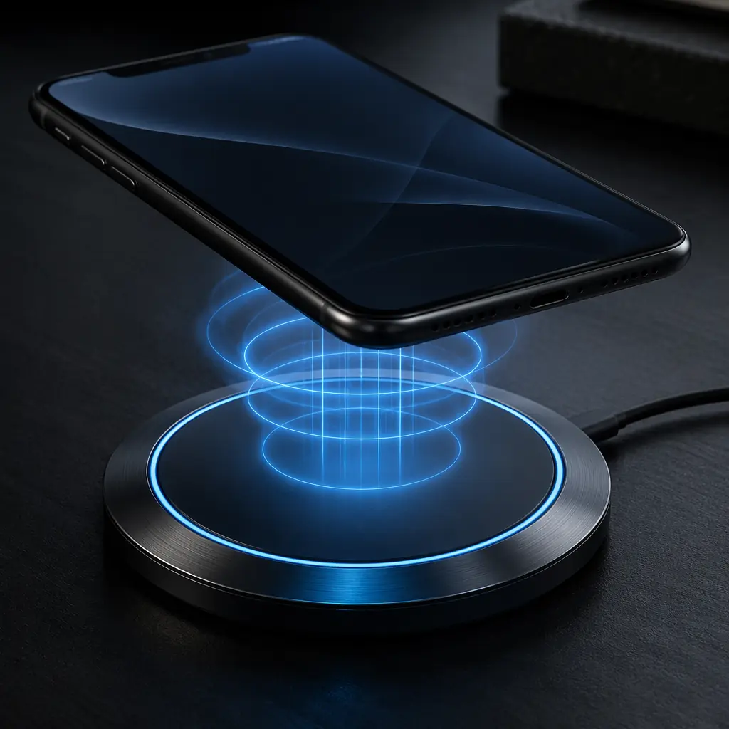
The wireless power transfer market is accelerating across three fronts: consumer (Qi2 chargers shipping in 500 million+ devices annually), industrial (automated guided vehicle wireless charging in warehouses), and automotive (SAE J2954 inductive charging for EVs at 11kW). What unites all three is the PCB — specifically, the transmitter and receiver coil boards, the inverter/resonant converter PCB, and the foreign object detection (FOD) and communication overlay. Your PCB is not just a carrier for components; it's the magnetic interface where kilowatts of power cross an air gap.
At Huaxing PCBA, we manufacture wireless power transfer PCBs for consumer electronics brands, industrial automation OEMs, and EV charging infrastructure suppliers across 9 countries. Our capabilities span the full WPT stack: single-layer coil PCBs with 4 oz copper for Qi transmitters, 4-6 layer FR-4 inverter boards with GaN FET switching at 6.78 MHz (AirFuel), and heavy-copper (6-10 oz) Litz-wire-integrated PCBs for EV wireless charging pads. Here's how to specify PCB manufacturing for each power level.
The PCB as a Magnetic Component: Planar Coil Design for Qi and AirFuel
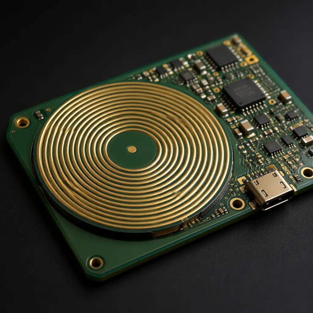
In a wireless power system, the transmitter and receiver coils are often implemented directly as PCB traces — a planar spiral coil etched into the copper layer. This eliminates a separate wound coil component, reduces BOM cost, and provides repeatable inductance (±3% vs ±10% for hand-wound coils). But it also means the PCB manufacturer is now manufacturing a magnetic component — and the copper thickness, trace width, and spacing tolerances directly affect the coil's quality factor (Q) and coupling coefficient (k).
Copper Thickness: 2 oz Minimum for Qi Transmitters, 4 oz for 15W+ Designs
The coil's AC resistance at the WPT operating frequency (110-205 kHz for Qi, 6.78 MHz for AirFuel) is dominated by skin effect and proximity effect — not DC resistance. At 200 kHz, the skin depth in copper is approximately 150 μm (6 mils). A 1 oz (35 μm) copper trace uses only 35 μm of the 150 μm skin depth, wasting two-thirds of the current-carrying capacity. 2 oz (70 μm) doubles the effective cross-section. For 15W Qi Extended Power Profile transmitters, we recommend 4 oz copper on the coil layer. Our copper weight selection guide includes the skin depth calculator for every frequency and copper thickness combination.
Trace Width and Spacing: 0.5mm Trace, 0.5mm Gap (Qi Baseline Profile)
The coil's inductance is determined by the number of turns, the trace width, the spacing between turns, and the outer diameter. For a Qi-compliant A11 transmitter coil (50mm outer diameter, 10 turns), the standard geometry is 0.5mm trace width with 0.5mm spacing. The PCB manufacturer must hold trace width tolerance to ±10% on the coil layer — a ±20% variation changes the inductance by ±8%, pushing the resonant tank out of the Qi specification and causing interoperability failures. We 100% verify coil inductance with an LCR meter on every production panel. See our impedance control guide for specifying inductance tolerances in fabrication notes.
Ferrite Shielding: Integrate During PCB Assembly, Not as a Post-Process
The planar coil on the PCB must be backed by a ferrite sheet (typically MnZn for Qi at 100-200 kHz, NiZn for AirFuel at 6.78 MHz) that shapes the magnetic field toward the receiver and shields the electronics behind the coil. The ferrite sheet is bonded to the back of the PCB using a thermally conductive adhesive — the assembly process must ensure zero air gaps between the ferrite and the PCB, as even a 0.1mm air gap reduces the coil inductance by 15-20% and increases stray field emissions. Our assembly line includes automated ferrite sheet lamination with vacuum pressing for bubble-free bonding.
Via Placement: Outside the Coil Area, Connected with Wide Traces
The inner and outer terminals of the planar coil must route to the resonant capacitor and inverter circuit through vias. These vias must be placed outside the coil area — any via inside the coil creates a local eddy current hot spot that reduces Q by 5-15%. The routing traces from the coil terminals to the vias must be at least 2x the coil trace width to avoid localized resistance increases. For multi-layer coils (common in AirFuel designs), the vias connecting the inner turns between layers must use 0.3mm drill with 0.6mm pad — any larger and the via ring encroaches into the magnetic field.
The Inverter/Resonant Converter PCB: Where the High-Frequency Switching Happens
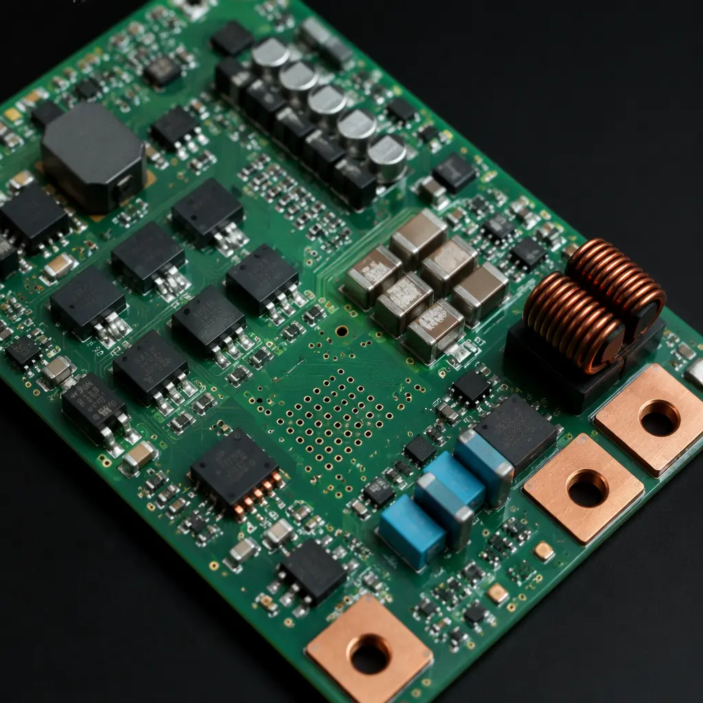
On the transmitter side, the inverter PCB converts DC input (5V USB, 12-24V industrial, or 400V EV battery) to the high-frequency AC that drives the transmitter coil. This is the most electrically demanding PCB in the WPT system — it combines high-frequency switching (110 kHz to 6.78 MHz), high current (up to 30A for 11kW EV charging), and the resonant tank's reactive power that can exceed the real power by a factor of 3-5x.
| Parameter | 5W Qi (BPP) | 15W Qi (EPP) | AirFuel Resonant (70W) | EV WPT (11kW) |
|---|---|---|---|---|
| Frequency | 110-205 kHz | 110-205 kHz | 6.78 MHz | 85 kHz |
| Switching device | Si MOSFET | Si MOSFET | GaN FET | SiC MOSFET |
| Layer count | 2-4 | 4 | 4-6 | 6-8 |
| Copper weight (power) | 2 oz | 2-3 oz | 3 oz | 6-10 oz |
| Resonant capacitor | SMD NP0/C0G | SMD NP0/C0G | SMD NP0 + film | Film capacitor bank |
| EMI standard | EN 303 417 | EN 303 417 | FCC Part 18 | CISPR 11 / SAE J2954 |
Key Takeaway: The resonant capacitor placement is the single most critical layout decision on the inverter PCB. The loop formed by the switching FETs → resonant capacitor → transmitter coil must have minimum area (< 5mm² loop for Qi, < 2mm² for 6.78 MHz AirFuel) to minimize radiated EMI. Use a solid ground plane on layer 2 (directly under the switching loop) to provide a low-inductance return path — a split or gapped ground plane under a WPT switching loop will radiate harmonics that fail FCC/CISPR emissions testing on the first attempt. Our EMC/EMI design guide covers the switching loop optimization rules.
EV Wireless Charging: The Heavy-Copper, High-Power Frontier
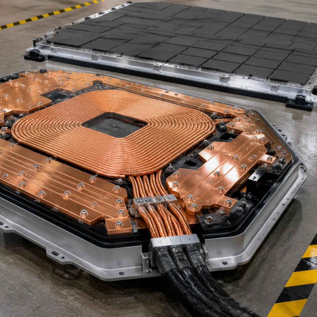
SAE J2954 defines three power levels for wireless EV charging: WPT1 (3.7 kW), WPT2 (7.7 kW), and WPT3 (11 kW). At 11 kW with 85 kHz operation, the transmitter pad PCB carries 30A RMS through the coil — requiring 6-10 oz copper that's far beyond standard PCB fabrication. But the real challenge is not just the copper weight; it's the integration of Litz wire terminations with the PCB and the thermal management of the ferrite core that sits between the coil and the aluminum shielding plate.
Litz Wire Integration: Soldered to Heavy-Copper PCB Pads
For EV-level power, a pure PCB coil would need impractical copper thickness (20+ oz). The industry solution is a hybrid: Litz wire for the main coil, terminated to heavy-copper PCB pads that carry the connection to the resonant capacitor bank. The terminations require 8 oz copper pads at least 15mm × 15mm with multiple thermal vias to a bottom-side heatsink plane. The Litz wire is hand-soldered or resistance-welded to these pads. Our heavy copper PCB guide covers the design rules for 6-10 oz inner and outer layers.
Ferrite Core Thermal Management: Keep Tc Below 120°C
MnZn ferrite cores in the EV transmitter pad experience core losses of 50-150W at 11 kW operation, heating the core to 100-130°C. The PCB underneath the ferrite must use a high-Tg laminate (≥ 170°C) to avoid delamination, and the copper ground plane under the ferrite should include thermal vias to conduct heat to an aluminum heatsink backplate. Our thermal management guide covers the via pattern density calculations for different heat fluxes.
Foreign Object Detection (FOD) Coil: A Second PCB Layer for Safety
SAE J2954 requires FOD to detect metallic objects (coins, paperclips, cans) between the vehicle pad and ground pad that could heat to dangerous temperatures. The FOD system uses an array of small sensing coils — typically implemented as a separate 2-layer PCB with 1 oz copper, with the coil array patterned on the top layer and a shield plane on the bottom. The FOD PCB sits directly above the main power coil PCB, separated by a thin (0.5-1mm) insulation layer. The manufacturing challenge is flatness — any warpage in the FOD PCB creates air gaps that degrade the magnetic coupling. We specify ≤ 0.5% warpage per IPC-TM-650 2.4.22 for all WPT PCBs. See our PCB warpage guide for the process controls that achieve this.
How to Specify Wireless Power Transfer PCBs: 6 Requirements Across All Power Levels
Coil Layer: 100% AOI + Inductance Measurement on Every Panel
The coil layer must pass 100% automated optical inspection (AOI) for trace width, spacing, and opens/shorts. Additionally, every production panel must have the coil inductance measured at the WPT operating frequency using an LCR meter — the reading must be within ±5% of the nominal value. Out-of-spec panels are rejected before component assembly. Our PCB testing guide covers all inspection methods.
Dielectric Strength: 1.5kV Hi-Pot Test Between Coil and Shield Layers
The isolation between the power coil (carrying up to 400V peak in EV applications) and the shield/ground layer must withstand 1.5kV AC for 60 seconds per IEC 60950-1. This requires a minimum dielectric thickness of 0.4mm for FR-4 (dielectric strength ≈ 20 kV/mm). Our high-voltage design guide covers the creepage and clearance requirements.
Surface Finish: ENIG for Flatness; OSP if Cost-Sensitive
The coil trace surface finish affects the AC resistance at high frequency — ENIG's nickel layer adds magnetic losses at 6.78 MHz that reduce Q by 3-8% compared to bare copper. For AirFuel designs at 6.78 MHz, we recommend OSP (Organic Solderability Preservative) on the coil layer for lowest AC resistance. For Qi designs at 100-200 kHz where nickel losses are negligible, ENIG provides the best flatness and shelf life. See our surface finish selection guide for the frequency-dependent loss data.
Solder Mask: Openings Over Coil Traces for Reduced Parasitic Capacitance
The solder mask over the coil traces adds a parasitic capacitance of 3-5 pF/cm² between adjacent turns, which detunes the resonant tank and reduces efficiency. For Qi and AirFuel designs, we recommend no solder mask over the coil area — leave the traces as bare copper with ENIG or OSP finish. For harsh-environment applications (outdoor EV pads), apply a thin (15-25μm) conformal coating instead of solder mask over the coil. Our solder mask guide compares the dielectric properties.
EMI Compliance: Pre-Compliance Scan Before Shipping
Every wireless power product must pass radiated and conducted EMI limits (EN 303 417 for Qi, FCC Part 18 for AirFuel, CISPR 11 for EV). We offer a pre-compliance EMI scan on every first-article WPT PCB — using a near-field probe and spectrum analyzer to identify switching harmonics above the limit before the product goes to the accredited test lab. This typically identifies 2-3 layout issues that, once fixed, result in a first-pass certification. See our EMC/EMI guide for the full pre-compliance checklist.
Traceability: Unique ID on Every WPT PCB for Interoperability Testing
The Qi and AirFuel certification programs require that each PCB variant tested is traceable to the specific production lot. We laser-mark a 2D data matrix with lot code, date code, and serial number on every WPT PCB — linking each certification test report to the exact production batch. Our FAI guide covers the complete traceability documentation.
Wireless Power Transfer PCB Trends: GaN, Higher Frequencies, and Multi-Device Charging
Three technology shifts are reshaping wireless power transfer PCB requirements:
GaN FETs Enabling Higher Frequencies: The transition from silicon MOSFETs to GaN (Gallium Nitride) FETs in WPT inverters reduces switching losses by 60-80% and enables operation at 6.78 MHz and 13.56 MHz for AirFuel resonant systems. GaN's fast switching edges (1-2 ns rise time) demand PCB layout with extremely low parasitic inductance in the gate drive loop — the gate driver must be within 5mm of the GaN FET, with a 4-layer PCB using layer 2 as a solid ground reference. Our signal integrity guide covers the high-speed layout rules that apply to GaN gate drivers.
Multi-Device Free-Position Charging: The Qi2 standard's Magnetic Power Profile (MPP) uses a magnetically-aligned single-coil design, but the next step is free-position charging — a surface where you can place multiple devices anywhere and they all charge simultaneously. This requires a PCB with an array of overlapping hexagonal coils, each individually driven, with complex multiplexing of the inverter to different coil subsets. The PCB becomes a multi-layer coil array with 6-8 layers and significant via density — similar to what we cover in our HDI PCB guide and via technology guide.
In-Flight Wireless Charging for Drones and Robotics: Industrial drones and warehouse robots are adopting wireless charging pads for autonomous opportunity charging — landing on a pad between missions for a 10-15 minute fast charge. These systems operate at 100-500W with tight size constraints, requiring the coil PCB to double as the mechanical landing surface. We apply an additional 0.5mm FR-4 stiffener layer and specify panelization optimization to handle the combined electrical and mechanical requirements.
Getting Started with Your Wireless Power Transfer PCB Project
Wireless power transfer PCB manufacturing spans the full range of PCB technology — from simple 2-layer Qi charger coils to 8-layer GaN-based AirFuel inverters to heavy-copper EV charging pads with integrated Litz wire and ferrite. The common thread is that the PCB is a magnetic component, not just an interconnect — and the manufacturing tolerances that are "good enough" for a digital PCB are not good enough for a resonant tank operating at 85 kHz or 6.78 MHz.
At Huaxing PCBA, we've manufactured wireless power transfer PCBs across all three power tiers — consumer (Qi, Qi2), industrial (AirFuel resonant, AGV charging), and automotive (SAE J2954 EV charging). Our in-house coil inductance verification (LCR on every panel), ferrite lamination (vacuum pressing for zero air gaps), and pre-compliance EMI scanning ensure your WPT PCB meets the certification requirements on the first submission. See our certifications or send your coil design files and inverter schematic to our engineering team for a 24-hour quote with WPT-specific DFM review.
