
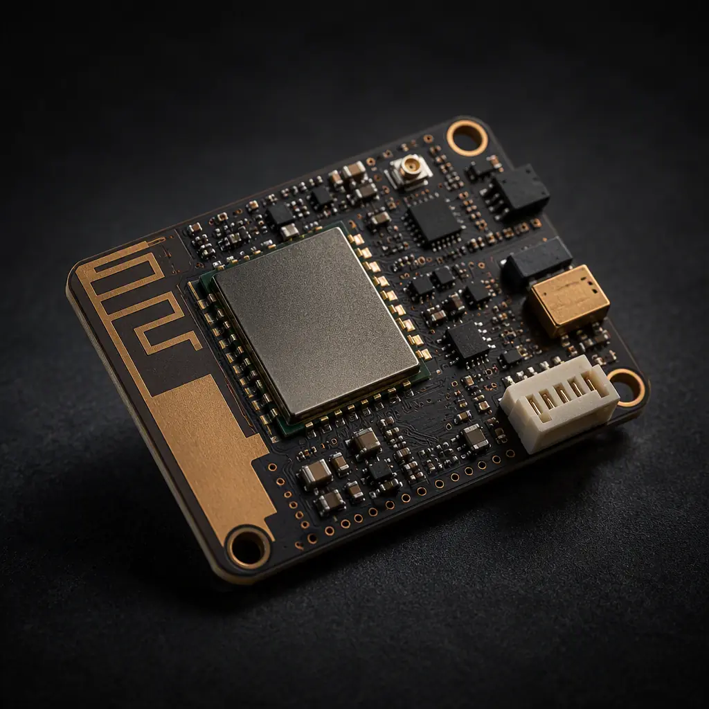
Every year, IoT hardware teams ship products that pass lab testing and then fail in the field with the same symptom: the device loses connectivity, drops registration, or transmits at reduced power. The root cause is rarely the module — Quectel, SIMCom, u-blox and other cellular modules are well-characterized. It is almost always the surrounding board: an antenna area with no keep-out, an RF trace routed over a split ground plane, a power supply that sags during the 2 A transmit burst, or a SIM interface with noise coupled onto the clock line. These are design decisions, and they are all fixable before the board goes to fabrication.
Huaxing PCBA builds and assembles connected product boards — including RF designs with controlled 50Ω impedance, hybrid FR-4/Rogers stackups, and 8 SMT lines that place 0201 components and LGA modules at 0.5 mm pitch — for customers shipping IoT products to 30+ countries under ISO 9001 and IATF 16949. This guide covers the design rules that determine whether your cellular IoT product actually works in the field.
LTE-M vs NB-IoT vs Cat-1 — Which Radio Goes on Your Board
The radio choice drives everything downstream: module footprint, antenna size, power budget, and certification path. LTE-M, NB-IoT, and Cat-1 are all 4G-based low-power technologies, but they differ sharply in throughput, mobility, and coverage behavior.
| Parameter | LTE-M (Cat-M1) | NB-IoT (Cat-NB1/NB2) | Cat-1 / Cat-1 bis |
|---|---|---|---|
| Downlink peak | ~1 Mbps | ~30–60 kbps | 10 Mbps |
| Uplink peak | ~1 Mbps | ~20–60 kbps | 5 Mbps |
| Bandwidth | 1.4 MHz | 200 kHz | 20 MHz (Cat-1bis: 1.4 MHz) |
| Mobility / handover | Yes | No (static) | Yes |
| Voice (VoLTE) | Yes | No | Yes |
| Typical use | Trackers, wearables, alarms | Meters, sensors, agriculture | Voice devices, video, gateways |
| Module cost | $$ | $ | $$$ |
For a battery-powered tracker that moves, LTE-M is the default. For a fixed water meter reporting a few times a day, NB-IoT wins on cost and coverage depth. For a device that needs voice or low-latency two-way communication, Cat-1 — or the single-antenna Cat-1 bis variant — is the practical floor. The board-level consequence is modest: all three operate in the 700 MHz–2.7 GHz band plan, so the antenna, RF routing, and power rules below apply across the board. If your product also carries a GNSS receiver for tracking, our GNSS receiver design guide covers the co-location rules for cellular plus GPS antennas.
Key Takeaway: LTE-M for moving assets, NB-IoT for fixed low-rate sensors, Cat-1/Cat-1 bis for voice or higher data. All share the same board-level RF and power design discipline — the radio choice does not change the layout rules.
Module Placement and Antenna Keep-Out Rules
Module vendors publish keep-out requirements in their hardware design guides, and they are not suggestions — the antenna efficiency loss from a violated keep-out is typically 2–6 dB, which translates directly into shorter range and worse indoor penetration. The antenna area is the single most important real estate on a cellular IoT board.
Respect the Antenna Keep-Out Zone — 10–15 mm Is Typical
Most LTE module vendors require a clear zone of 10–15 mm around the antenna pad or connector, with no copper on any layer, no components, and no traces crossing underneath. The exact value is in the module's hardware design guide — check it for your specific module. Ground pour directly under the antenna pad detunes the radiator and shifts the resonant frequency; if the vendor allows a ground plane below the antenna, follow their stated distance precisely.
Place the Module Close to the Antenna — Short RF Trace Wins
Route the RF path from module to antenna as short as possible — under 20 mm is a good target for a 50Ω trace, and many designs put the antenna on the same board edge as the module. Every millimeter of RF trace adds loss, and every via adds a discontinuity. If the antenna is external (via a U.FL/IPEX connector), place the connector within 15–20 mm of the module's antenna pad.
Keep Digital, Power, and High-Current Nets Out of the RF Zone
Do not route the DC-DC switch node, the battery charge path, or high-speed digital lines (USB, SDIO) near the antenna area. The transmit burst of the cellular radio (up to 23 dBm, or 200 mW, plus harmonics) couples into unshielded digital lines, and digital switching noise couples back into the receiver — reducing sensitivity exactly when the device is far from a tower.
Routing the RF Signal — 50Ω Controlled Impedance
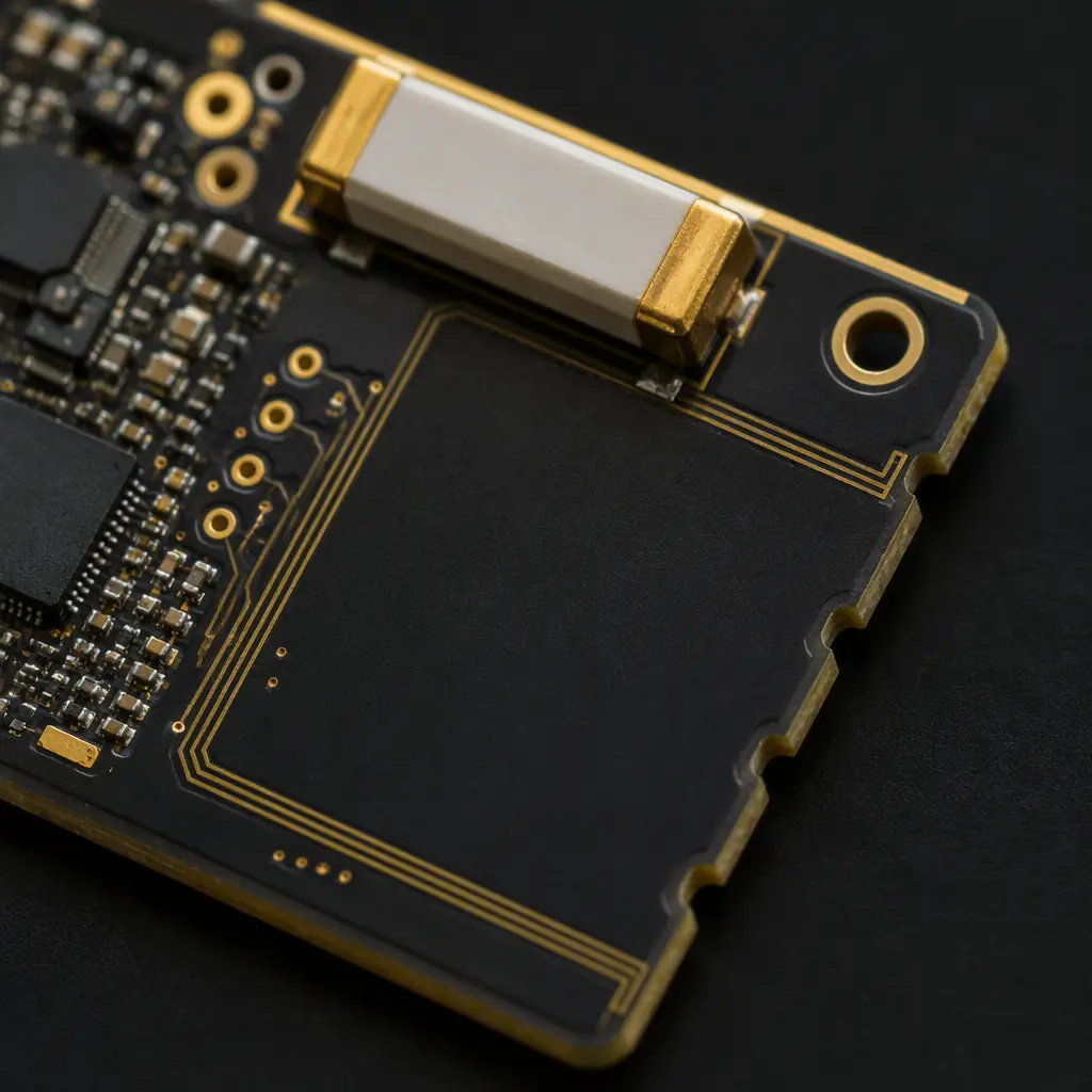
The trace between the module's antenna pad and the antenna is a transmission line and must be controlled to 50Ω single-ended. The impedance is set by the trace width, the dielectric height to the reference plane, and the ground structure around it.
Use Coplanar Waveguide With Ground (CPWG) on an Outer Layer
The standard structure for a cellular RF trace is a 50Ω coplanar waveguide with ground: a trace on an outer layer, solid ground plane directly below, and ground pours on both sides of the trace with a defined gap. Keep the trace on the top layer next to the module, avoid vias, and avoid routing on an inner layer (buried stripline is harder to control and adds vias). Specify this net class in the fabrication notes with a ±10% tolerance, or tighter if the module vendor asks. Our impedance control guide covers how impedance is calculated and verified at the fab.
Add Stitching Vias Along the RF Trace
Ground the coplanar pours with stitching vias every 50–100 mils along both sides of the trace. This keeps the coplanar ground at the same potential across the trace length and prevents the pour from resonating. On a 2-layer board, this is especially important because the ground reference is weaker.
Reserve a Pi-Matching Network — Even If You Think You Don't Need It
Module vendors recommend a pi-network (series inductor/cap plus two shunt components) between the module and the antenna to tune out board parasitics and antenna impedance mismatch. Reserve the pads even if you plan to populate zero-ohm or leave them empty — adding a matching network after the fact on a production board requires a respin. Measure with a VNA at the antenna connector and tune the values during bring-up.
Material Choice — FR-4 Is Usually Fine, With One Caveat
Cellular bands span 700 MHz to 2.7 GHz. On short RF traces (under 20 mm), standard FR-4 with controlled impedance is perfectly adequate — the loss at these frequencies is manageable. The caveat is consistency: specify impedance-controlled fabrication so the width is tuned to your actual stackup, and for higher bands (B42/B43 TDD at 3.4–3.8 GHz, CBRS) consider low-loss materials. For boards mixing RF and very high-speed digital, hybrid stackups with Rogers or PTFE on the RF layers are an option — see our PTFE high-frequency manufacturing guide for the material handling realities.
Power Supply Design for Transmit Bursts
A cellular module is not a steady-state load. During a transmit burst, the module draws current in a sharp pulse — up to 2 A for GSM-class bursts, and typically 0.5–1.5 A for LTE-M/NB-IoT/Cat-1 depending on power class and band. If the supply voltage sags below the module's minimum (often 3.3 V or 3.4 V), the module de-rates its transmit power, and range drops silently.
Size the Input Capacitance for the Burst, Not the Average
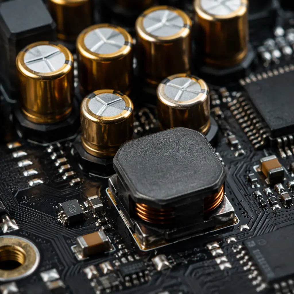
Place a low-ESR bulk capacitor (33 µF or 47 µF, X5R/X7R) plus 10 µF and 100 nF ceramics directly at the module's VBAT pins, within 5–10 mm. The bulk cap supplies the burst current between DC-DC converter response cycles; without it, the module sees voltage droop on every transmit. Check the module datasheet's recommended capacitance — most vendors specify a minimum total capacitance at the power pin.
Verify the DC-DC Converter's Transient Response
A converter sized for the average current (e.g., 300 mA for an NB-IoT module) will droop during the 1 A burst. Size the converter for the peak burst current plus 30–50% margin, and check its load-transient spec — a converter with 100 mV droop on a 100 mV step might be fine for a sensor but marginal for a radio. During bring-up, measure the VBAT waveform with a scope at max TX power and confirm droop stays under the module's spec.
Route the Power Path Wide and Direct
Use wide traces or a dedicated power pour for VBAT — 30–50 mils minimum per amp — and avoid daisy-chaining the module's power through other circuits. Keep the DC-DC converter's switching loop (input cap, inductor, output cap) tight and away from the RF trace and antenna area. Our power integrity guide covers decoupling and plane design in depth.
SIM/USIM Interface, Grounding and EMI Shielding
SIM interface problems are a top field-failure category for cellular IoT devices: a device that intermittently loses registration or fails to attach is often a SIM clock line picking up noise, or a SIM socket with marginal ESD protection.
Route SIM Lines With Ground Guarding and ESD Protection
Route the SIM clock, data, and reset lines with a ground trace or pour between them, keep the traces short (under 20 mm), and avoid routing them near the RF trace or DC-DC switch node. Add a low-capacitance TVS array (1–2 pF) at the SIM socket, and series resistors of 22Ω on the clock and data lines if the module reference design calls for them. Follow the module vendor's pull-up and pull-down requirements on the reset and presence lines.
Solid Ground Under the Module — No Splits, No Excuses
The area under the module must have a continuous ground plane on the adjacent layer, with ground vias around the module's ground pads. Module vendors specify a ground via pattern in their reference designs — copy it. Splits in the ground plane under the module turn it into a slot antenna and wreck both emissions and receiver sensitivity. For designs with analog or sensor sections, see our mixed-signal grounding guide.
EMI Shielding — Can, Gasket, or Careful Layout
If the product must pass radiated emissions or immunity testing (FCC/CE/PTCRB), a shield can over the module is the most reliable option, with a perimeter of ground pads and vias under the can footprint. If a can is not possible, keep the module away from board edges and user-facing connectors, and keep the antenna feed line as short as possible. Our EMI/EMC design guide covers emissions control strategies for certified products.
Manufacturing Considerations for Module Boards
Module boards are dense, mixed-technology assemblies — LGA modules, chip antennas, and fine-pitch passives on the same board as a battery connector and a USB port. A few manufacturing choices have outsized impact on yield and field reliability.
LGA Module Pads — Via Placement and Solderability
LGA modules (the most common form factor for LTE-M/NB-IoT) have pads on the bottom face with no balls. Put the escape vias outside the pad or use via-in-pad with filled and capped vias — a plain via inside the pad wicks solder away from the joint during reflow. The module's thermal/power pads should have a small array of thermal vias with proper tenting on the bottom side. Our via fill types guide explains filled vs plugged vs tented options.
Stencil Design for Mixed-Pitch Boards
Module boards mix 0.5 mm-pitch LGA pads with 0201/0402 passives and a chip antenna. The stencil thickness is a compromise: step-stencils (two thicknesses on one stencil) are common for these boards so the fine-pitch module pads get less paste than the power components. Ask your assembler for a step-stencil review during DFM — it is a standard part of our quoting process. See our stencil design guide for aperture rules.
X-Ray Inspection for LGA and Shielded Modules
LGA solder joints are not visually inspectable, and shield cans hide the module entirely. Specify X-ray inspection of the module pads — ideally 100% on the first article and a sample per batch afterward. If your assembler cannot X-ray LGA modules, that is a red flag for this board type. Our inspection methods guide compares X-ray with AOI and SPI coverage.
Summary: The Board Around the Module Is the Product
Cellular IoT failures in the field are overwhelmingly board-level: antenna keep-out violations, uncontrolled RF traces, power droop during transmit bursts, and noisy SIM interfaces. Each has a design rule and a fabrication requirement — respect the antenna zone, control the 50Ω path, size the burst capacitance, guard the SIM lines, and verify the assembly with X-ray. Get those right and the module does what it is specified to do.
At Huaxing PCBA, we fabricate impedance-controlled boards with ±5% targets, assemble LGA and castellated modules across 8 SMT lines with X-ray verification, and support hybrid RF stackups for connected products. Read our IoT PCB design guide for the broader connectivity picture, or send your module reference design and layout to our engineering team for a free DFM and impedance review with your 24-hour quote.
