
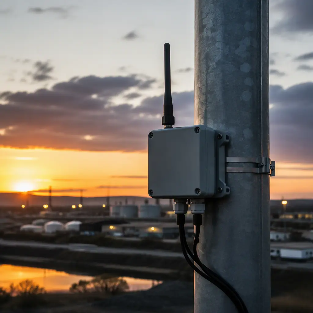
LoRaWAN has become the default wireless standard for long-range, low-power IoT: utility meters, agricultural soil sensors, warehouse trackers, and smart-city infrastructure all run on 868 MHz (Europe) or 915 MHz (North America) sub-GHz links. The radio can reach -137 dBm sensitivity at the lowest spreading factor — which means a well-laid-out node talks to a gateway kilometers away on milliwatts of power. But that range is only achievable if the PCB around the transceiver is designed correctly: a poor RF layout can cost 10-20 dB of link budget, which is the difference between 5 km and 500 m.
Huaxing PCBA manufactures sub-GHz IoT boards for metering, agricultural, and industrial customers — controlled-impedance FR-4 and high-frequency laminates, 2-32 layer stackups with 3/3 mil capability, impedance tolerance to ±5%, and 8 SMT lines with AOI, X-ray, and RF test support. This guide walks through the RF front-end, antenna selection, matching, battery-life design, and the DFM requirements you should put on the fabrication drawing.
Why Sub-GHz Layout Differs From 2.4 GHz Design
Most hardware engineers have designed a 2.4 GHz BLE or Wi-Fi board at some point. Sub-GHz design feels deceptively easier because the frequency is lower — but the physics changes the rules in ways that surprise people.
The Wavelength Is 10 Times Longer
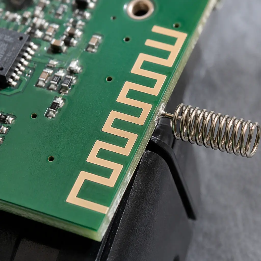
At 868 MHz the free-space wavelength is about 345 mm — a quarter-wave antenna is roughly 86 mm long. That is far too long to fit as a straight trace on a small sensor board, which is why sub-GHz boards use meandered trace antennas, chip antennas, or external spring/whip elements. The long wavelength also means the antenna interacts with the whole board and its enclosure, not just a small keep-out zone.
Component Parasitics Scale With Frequency
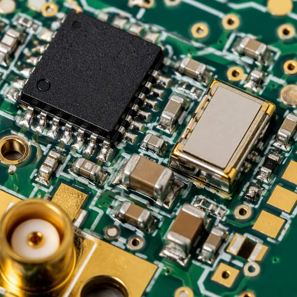
At 868 MHz, a 0402 capacitor's parasitic inductance is still significant, and a badly placed ground via can add several nH that detunes the matching network. The RF section needs the same discipline as a 2.4 GHz design: short traces, solid ground reference directly under the RF path, and vias placed right at the pad of every ground pin.
The Receiver Is Extremely Sensitive — and Extremely Vulnerable
A LoRa receiver at -137 dBm is working with signals a million times weaker than a typical BLE receive level. Noise coupling from the digital section, switching regulators, or the MCU clock that would be invisible on a BLE board can desensitize a sub-GHz receiver. Power supply filtering and layout separation are not optional.
Key Takeaway: Lower frequency does not mean easier layout. The RF section of a sub-GHz board needs the same care as a 2.4 GHz design, plus attention to antenna size, ground-plane interaction, and receiver sensitivity that the higher-frequency world rarely worries about.
The RF Front End: Transceiver, SAW Filter, and Matching
Most sub-GHz designs are built around a Semtech SX1261/SX1262-class transceiver or a module integrating one. The transceiver's reference design gives you the schematic; the layout is where range is won or lost. Our IoT PCB design guide covers the system-level architecture these radios sit inside.
Follow the Reference Design for the RF Matching Network
The SX1262 datasheet specifies a balun and LC matching network between the differential RF pins and the 50 Ω antenna path, tuned for the operating band. Use the exact component values for your band (868 or 915 MHz differ), place them in a tight cluster, and do not "optimize" the values by guesswork — tuning comes later with a network analyzer. The matching components must sit close to the transceiver with their ground pins tied to the same continuous ground pour.
Add a SAW Filter if Your Product Must Pass EMC Testing
A SAW filter after the radio cleans up out-of-band emissions and improves rejection of strong nearby transmitters (for example, cellular bands near 868 MHz). It costs about 20-30 cents and a little insertion loss (~2 dB), but it is the difference between passing ETSI EN 300 220 harmonic limits on the first try and redesigning the output stage. For cost-sensitive high-volume designs, evaluate whether the transceiver's own harmonic performance is sufficient before adding it.
Route the 50 Ω Feed as a Coplanar Waveguide
The antenna feed from the matching network to the antenna or connector should be a controlled 50 Ω trace. On 1.6 mm FR-4, a grounded coplanar waveguide (CPWG) with a ~1.2-1.5 mm trace and 0.25-0.4 mm gaps to ground pours on both sides is a practical geometry, with ground stitching vias along the trace every 3-5 mm. Specify ±10% impedance control (Huaxing holds ±5%) and verify with TDR on first articles. Our impedance control guide explains the stackup and coupon requirements.
Key Takeaway: The RF chain is: transceiver → balun/matching → optional SAW filter → 50 Ω CPWG feed → antenna. Each transition must be tight, grounded, and impedance-controlled, or the sensitivity number on the datasheet will never appear in the field.
Antenna Options for Sub-GHz Boards
Antenna choice is the highest-leverage decision on a LoRaWAN node. It determines size, cost, range, and how much engineering effort the tuning phase takes. See our PCB antenna design guide for the full design methods; the table below summarizes the options for sub-GHz.
| Antenna Type | Typical Size | Gain / Efficiency | Best For |
|---|---|---|---|
| Meandered PCB trace (quarter-wave) | ~86 mm path, folded | -3 to -1 dBi, narrow band | High-volume, low-cost sensors |
| Chip antenna | 9-25 mm × 3-8 mm | -4 to -1 dBi, needs clearance | Compact boards, moderate range |
| Spring / whip (helical) | 20-50 mm tall | -2 to +1 dBi | Trackers, handhelds, plastic enclosures |
| SMA + external antenna | Connector + external | 0 to +3 dBi | Gateways, fixed installations, maximum range |
Trace Antennas Need a Clean Ground Plane Below
A meandered quarter-wave trace antenna radiates against the board's ground plane — the ground plane is literally half the antenna. The antenna must sit on a board edge or corner with the ground pour beneath it intact, and a clearance of 3-5 mm around the trace with no copper, traces, or components. The feed point connects to the 50 Ω line; the far end is open. Tuning is done by trimming the last segment or adjusting the matching network.
Chip Antennas Are Easy to Place, Hard to Get Right
Chip antennas shrink the board but impose strict datasheet rules: a specific ground clearance area, a specific location (usually a board corner), and a required matching network. Ignoring the clearance rule can cost 5-8 dB. Always copy the datasheet's recommended PCB layout verbatim — including the ground cutout, if one is specified.
Gateways Should Never Rely on a PCB Antenna
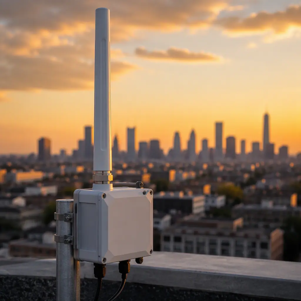
A gateway's range covers the whole network, so its antenna is the worst place to save money. Use an SMA connector and a proper external antenna (collinear or panel with 2-6 dBi gain), mounted away from the enclosure metal. The connector needs a solid RF launch: keep the 50 Ω trace from the connector to the concentrator short, and ground the connector body with multiple vias.
Layout Rules: Placement, Keep-Outs, and Grounding
The mechanical layout of the RF section follows a small set of non-negotiable rules. Our RF PCB manufacturing guide covers the fabrication side of the same discipline.
Keep the RF Section in Its Own Corner, Away From Noise Sources
Place the transceiver and its antenna at one edge of the board, far from the MCU, switching regulator, and any high-current traces. If the board has a metal shield can, it should surround only the RF section. Digital signals must not cross under the antenna area or the 50 Ω feed on any layer.
Ground Stitch Everything Around the RF Path
Every ground pad of the transceiver, SAW filter, and matching components gets its own via to the main ground plane, placed directly at the pad. Along the CPWG feed, add stitching vias on both sides every 3-5 mm. This keeps the return current on a tight path under the signal trace and prevents the ground plane from becoming a radiating structure itself.
Isolate the Switching Regulator From the Radio
The DCDC converter that powers the node is the biggest noise source on the board. Keep its switching node (the inductor connection) short and far from the RF section, use a dedicated ground pour for the converter that connects to the main plane at one point, and place the RF supply filter (ferrite bead plus bulk and RF capacitors) right at the transceiver's supply pin. Our power integrity guide covers supply filtering in detail.
Battery Life: Designing for 5-10 Years on One Cell
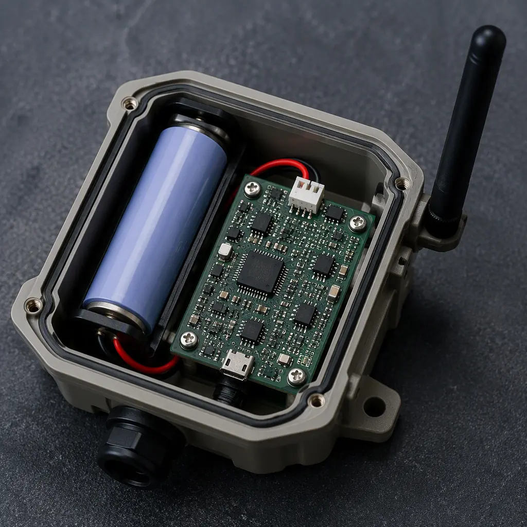
The second half of a LoRaWAN product is power: most nodes are battery-powered and must run for years. The radio only transmits for milliseconds at a time — the average current is set by sleep current and duty cycle, not by the transmit burst.
Work From a Real Duty-Cycle Budget
A typical metering node transmits a 46 ms packet at +14 dBm (~40-100 mA depending on the radio and supply) every 10 minutes. At a 2 µA sleep current, the average current is roughly 10 µA — dominated by sleep, not transmit. A 3.6 V Li-SOCl2 cell (ER18505, ~3800 mAh) then delivers 5-10+ years. Change the interval to 1 minute and the transmit term starts to dominate: the same cell drops to roughly 1-2 years. Model your own numbers before choosing the cell.
Minimize Sleep Current at the Schematic Level
Sleep current is a sum of many small leaks: regulator quiescent current, pull-up resistors left energized, leakage into unpowered ICs, and the MCU's own deep-sleep draw. Use a low-quiescent LDO or a DCDC with <2 µA quiescent current, switch power domains with MOSFETs or load switches, and check every pull-up resistor — a single 100 kΩ pull-up to 3.3 V wastes 33 µA permanently, which alone can cut battery life in half.
Watch the Transmit Current Path
At +22 dBm (the SX1262's high-power setting), the transmit current can exceed 100 mA. The supply trace and battery contacts must carry this without voltage sag — a 0.5 Ω contact resistance costs 50 mV under load, and brownouts at the end of battery life are a classic field failure. Keep the battery-to-regulator path short and wide, and use gold-plated contacts rated for the peak current.
Key Takeaway: Battery life is decided by microamps, not milliamps: sleep current and duty cycle dominate. Choose the cell from a real duty-cycle budget, and hunt down every microamp of leakage at the schematic review stage.
Certification: ETSI EN 300 220 and FCC Part 15.247
Before a LoRaWAN product can be sold, it must pass regional radio certification. The PCB design directly affects how painful that process is.
Know Which Rule Applies to Your Band
Europe's 868 MHz band falls under ETSI EN 300 220 (with a 1% duty-cycle limit for many channels), while the US 915 MHz band operates under FCC Part 15.247. Both limit radiated emissions, harmonics, and spurious output. The layout decisions that matter: a clean output stage (SAW filter, good grounding), a matching network that presents the right load to the PA, and an antenna feed that does not radiate harmonics.
Use a Certified Module to Shorten the Path
If time-to-market dominates, use a pre-certified LoRaWAN module (SX1262-based modules with FCC/CE approval are widely available). The end product still needs some testing — enclosure effects, power supply — but the radio portion is largely covered. If you integrate the bare transceiver, budget for conducted and radiated testing with a pre-compliance lab before the full certification run.
Design for Testability From the Start
Add RF test points (a 50 Ω pad in the feed line, or a small probe pad after the matching network) so the lab can measure conducted output power and harmonics without modifying the board. On the production side, an RF functional test — transmit power and frequency check on every unit — catches assembly defects before they reach the field. Our testing methods guide places RF tests in the full production test strategy.
DFM for Sub-GHz Boards: What to Put on the Drawing
A sub-GHz board is usually a modest 2-6 layer design, but the RF section imposes requirements that a standard digital fab drawing may not cover. Specify these explicitly:
Impedance Control on the 50 Ω Feed and Coupons Per Panel
Request ±10% impedance control on the antenna feed (tighter if you designed for it), with coupons on every panel and reported measurement data. The coupon must mirror the actual stackup — same dielectric, same trace geometry. Do not accept "impedance verified" without numbers. Our stackup design guide covers how to define this correctly.
Controlled Dielectric and Copper Weight
The antenna feed's impedance depends on the dielectric constant of the laminate. Specify FR-4 with a known Er (4.2-4.5) or a controlled-Dk material for the RF layer, and fix the copper weight (typically 1 oz for the signal layer). If the design uses a high-frequency laminate for the antenna area, the fab must know which layers use which material — mixed-stackup RF boards are routine for us.
Keep the Antenna Area Free of Solder Mask and Silkscreen
Solder mask over the trace antenna shifts its resonant frequency — specify mask removal (or a mask opening) over the antenna element, and keep silkscreen and component identifiers out of the keep-out zone. If the board uses a castellation or edge connector for a whip antenna, note the plating and edge requirements. Our solder mask guide explains the options.
Summary: The LoRaWAN Node Checklist
A LoRaWAN node that delivers its datasheet range is designed with the RF section isolated at a board edge, a SAW-filtered and matched front end, a controlled-impedance 50 Ω feed, an antenna with a clean ground plane and clearance, a power budget dominated by a few microamps of sleep current, and a fabrication drawing that specifies impedance coupons, controlled dielectric, and mask-free antenna areas. On the assembly side, RF functional test on every unit catches the defects that range testing in the field would otherwise find months later.
At Huaxing PCBA we manufacture sub-GHz IoT boards up to 32 layers with controlled-impedance capability to ±5%, mixed FR-4 and high-frequency laminates, 3/3 mil fine-line routing, and full RF assembly support — 8 SMT lines, X-ray for shield cans and connectors, and flying-probe plus functional testing. Our DFM review checks the RF stackup, impedance coupons, antenna keep-outs, and assembly requirements before tooling. Read our cellular IoT module guide to compare LPWAN options, or send your files for a free DFM review and quote.
