
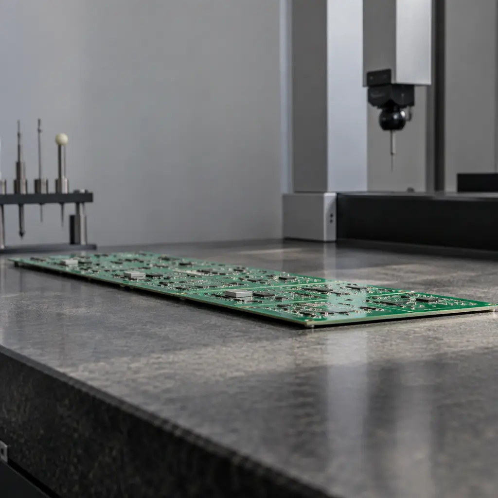
Flatness sounds like a simple property of a board, until you have to hold one to a number. Two defects account for almost every flatness dispute between a fabricator and a buyer: bow and twist. They look similar on a table and behave completely differently in a stencil printer, a reflow oven and a test fixture. The standards treat them as separate characteristics with separate limits precisely because they fail differently. An incoming inspection that measures one and not the other, or measures both against the wrong limit, is measuring nothing useful.
This guide covers both defects: what each one physically is, the IPC-6012 acceptance values a buyer can actually hold a supplier to, how to measure flatness so the number is meaningful, why the right limit depends on how you will assemble the board, and how to write bow and twist into the purchase order. It sits alongside our PCB manufacturing tolerances guide, which covers dimensional tolerance as a whole, and our PCB warpage prevention guide, which addresses the process side. Here the focus is the delivered board and the spec you put around it.
At Huaxing PCBA we inspect flatness as a routine outgoing control across 8 SMT lines under IATF 16949 and ISO 9001, and we measure bow and twist against IPC-6012 by board class, not by a single blanket figure. The limit is written into the inspection plan and tied to how the customer's assembly line will actually run.
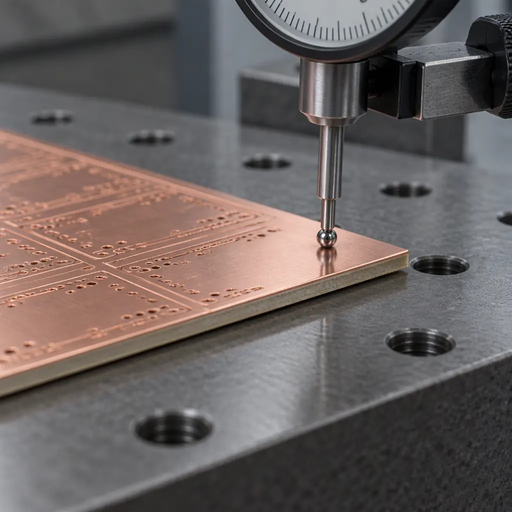
Bow and Twist Are Not the Same Defect
Both are deviations from flatness, and that is where the similarity ends. The distinction matters because the standard gives them the same numeric limit but a different geometry, and because the two deformations put stress on different parts of an assembly.
Bow is a cylindrical deformation — the board curves like a shallow arch along one axis, so the corners lift in a single direction while the surface is developable. A bow makes the board rock along one edge like a rocking horse. In a stencil printer, that rocking motion is what causes inconsistent paste deposition from one end of the panel to the other, because the squeegee sees a gap that varies along the print stroke.
Twist is a saddle deformation — the board warps around two axes at once, so two diagonally opposite corners lift and the other two drop. Twist is the more damaging of the two for assembly because no three points sit coplanar together; the board never settles flat on a fixture, a conveyor or a platen. A twisted panel on a conveyor rail can lift a corner into the path of a nozzle or a nozzle into the board, and a twisted board on a test fixture can fail to make contact on the high pins and over-stress the low ones.
Key Takeaway: Bow is a single-axis curve; twist is a two-axis saddle. They share a numeric limit in the standard but fail the assembly line differently. Always measure both, and specify both — a board can pass bow and still twist, and twist is the one that jams a conveyor.
The IPC-6012 Acceptance Limits
The limits come from IPC-6012, which governs qualification and performance for rigid boards, and the measurement method from IPC-TM-650. The headline numbers are simple, but the nuance is in which one applies.
| Board use / class | Bow and twist limit | Comment |
|---|---|---|
| Surface-mount (SMT) boards — general | 0.75% | The default for boards that go through stencil printing and reflow |
| Non-SMT boards / other applications | 1.5% | Boards with no fine-pitch surface-mount requirement |
| Boards for BGA / fine-pitch attach | 0.5% | Often specified by the customer in addition to the class limit |
| Measurement method | IPC-TM-650, method 2.4.22 | Measured across the panel or coupon as specified |
The limit is expressed as a percentage, not a distance, which is the detail most buyers miss. Bow and twist are calculated as the maximum deviation from a reference plane divided by the length of the side being measured, times 100. That means the same physical curve is a smaller percentage on a long board than on a short one, and a 0.75% limit permits about 1.5 mm of deviation on a 200 mm board but only 0.75 mm on a 100 mm board. When you write a limit, write the percentage and the measurement direction, not a millimetre figure, or the spec is not reproducible.
How to Measure Flatness So the Number Means Something
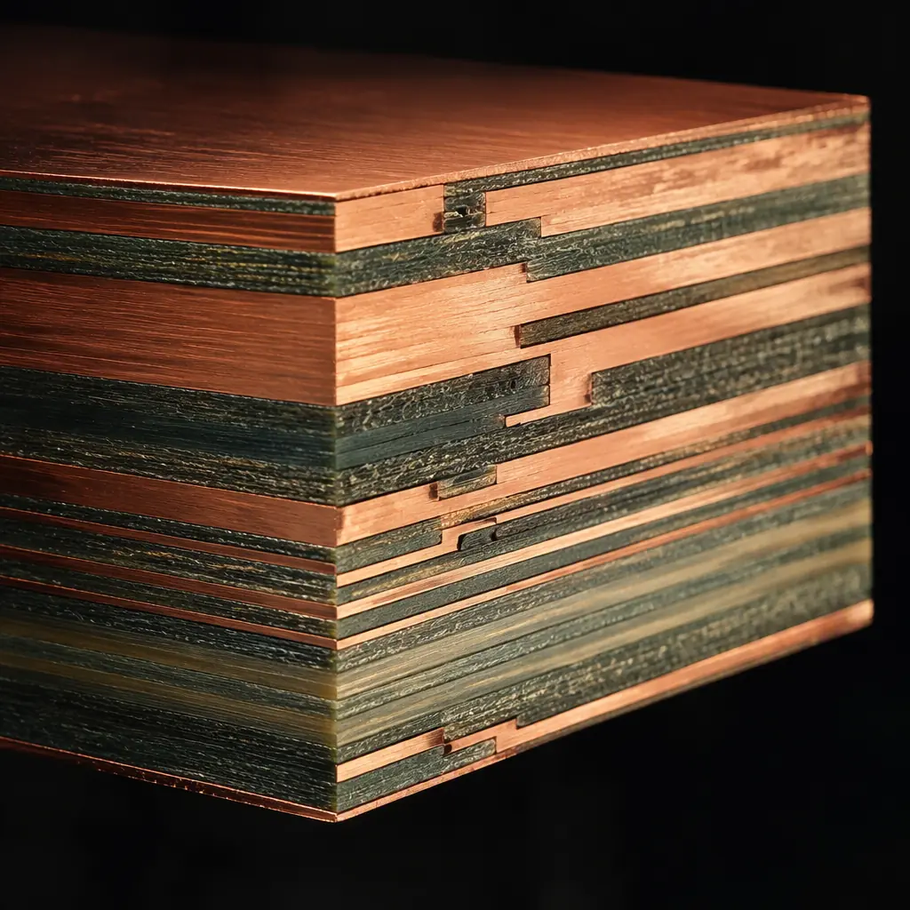
A flatness measurement is only as good as the reference plane it is taken against. Three setup decisions decide whether two results are comparable.
The seating plane. Bow and twist are measured against a reference surface the board rests on. The standard method places the board on a flat plate and measures the lift of the corners and edges, or the maximum gap between board and plate. If one inspector measures the lift of a single corner and another measures the maximum gap anywhere on the panel, the two numbers will not match even on the same board. Fix the method to the standard clause and use it every time.
Support and free state. A board measured while supported differently, or measured while still under the influence of a previous process, will give a different answer. Measure in the free, unrestrained state on a flat reference surface, at a defined temperature, and let the board stabilise first. A board measured warm off a press or a coating oven can show a transient flatness that is not the delivered condition.
Sample and location. On a panel with many boards, decide whether the specification applies to the panel or to the individual board, and measure at the same locations each time. Measuring the worst corner of one panel and the best corner of the next tells you nothing about the process. Define a fixed set of measurement points and report the maximum.
Getting the measurement right matters because the measurement is the only thing that makes the limit enforceable. See PCB incoming quality inspection for how flatness sits alongside the other first-article and receiving checks, and PCB test coupon design for how coupons can carry some of these measurements alongside the board.
Why the Right Limit Depends on Your Assembly Line
The standard gives a default, but the correct limit for a given board follows from what the board will go through. A limit chosen without reference to the process is either too loose to protect the build or too tight to be economic.
A board that will be stencil-printed and reflowed needs a tight limit because the printer relies on the panel seating flat against the tooling. A board that will be hand-soldered or wave-soldered through holes can tolerate more, which is why the non-SMT figure is looser. A board carrying a large BGA or a fine-pitch package needs a tighter limit still, because the coplanarity of the package balls over a warped board is what decides whether the joints form; that is why 0.5% is commonly added on top of the class limit for BGA attach. The board must be flat enough for the last and most demanding step in the process, not the first. See PCB stackup design for how the layer construction feeds into flatness from the design side.
What Causes Bow and Twist
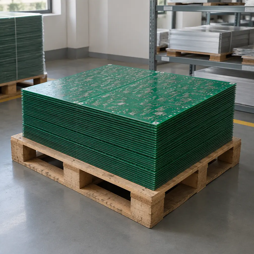
Bow and twist are not random. They come from the same root cause in almost every case: asymmetry. When the layers on one side of the board behave differently from the layers on the other, the board builds in a locked-in stress that it releases as a curve.
Unbalanced copper distribution
If one side of the stackup carries more copper area than the other, the two sides expand and contract differently through the heat of lamination and reflow. The result is a board that curls toward the copper-light side. Copper balancing — keeping the total copper area per layer roughly balanced across the stackup — is the single most effective design-side control. See PCB stackup design.
Asymmetric stackup and unbalanced build-up
A stackup that is not symmetric about the centre line builds in a bend. Even where symmetry is impossible for electrical reasons, keeping the materials and copper weights as symmetric as the design allows minimises the locked-in stress. A hybrid stackup mixing different laminate types is especially prone to this.
Material choice and glass transition temperature
Lower-Tg materials soften earlier and move more through the thermal cycle of assembly, so they twist more than higher-Tg materials in the same construction. Where flatness is critical through a high-temperature reflow, a higher-Tg laminate or a more dimensionally stable material pays for itself. See PCB laminate selection.
Panelisation and panel geometry
How the boards are laid out on the fabrication panel affects flatness after depanelisation. A layout that puts large areas of bare laminate next to dense boards, or a panel that is long and narrow, can twist more than a compact, balanced one. Strong, well-placed break-away tabs hold the panel flat and release cleanly. See PCB depanelisation methods.
Process steps: pressing, drilling and thermal history
Lamination press parameters, the number of thermal cycles and any stress-relief baking all feed into the final flatness. A board that is flat off the press but not stress-relieved can twist after reflow. This is one reason flatness should be measured after the board is in its delivered, stable state rather than straight off an intermediate step.
Thinner boards and larger formats
Flatness is significantly harder to hold on thin boards — below about 0.8 mm, and especially in the 0.4-0.6 mm range — and on large panels. Thin cores flex under their own weight in handling and are far more sensitive to copper imbalance. If you need a thin board flat, expect tighter process control and possibly a stiffer construction or a carrier. See PCB board thickness selection.
Procurement tip: Bow and twist are almost always a design and construction issue, not a fabricator's mistake. If you get boards that fail flatness, the fastest route to a fix is usually to ask about copper balance and stackup symmetry rather than to ask the fabricator to press harder. A fabricator who can walk you through the balance of your stackup is one whose flatness numbers you can trust.
Writing Bow and Twist Into the Purchase Order
A flatness requirement that is not in the purchase order is not a requirement. Specify it the same way you would specify a tolerance, with the value, the method and the sampling named.
State the percentage and the class
Name the limit as a percentage of the measured side, name the IPC-6012 class the board is built to, and state whether the SMT figure (0.75%) or a tighter BGA-attach figure (0.5%) applies. Do not write a millimetre figure without the board dimension it corresponds to.
Name the measurement method and the reference plane
Cite IPC-TM-650 method 2.4.22, state that measurement is on a flat reference surface in the free state, and name the temperature at which the board is measured. This is what makes your limit reproducible across suppliers and over time.
Define the sampling plan
Say whether the limit applies per panel or per board, how many samples per lot are measured, and what the accept/reject rule is. A limit with no sample plan cannot be enforced on a lot. See PCB AQL sampling for how to set an inspection level.
Require flatness data in the inspection report
Add bow and twist measurements to the documentation you require with the shipment, so the number is recorded rather than asserted. See PCB test report documentation for how these measurements sit in the report package, and the specification and RFQ guide for how the clause fits with your other requirements.
Summary: Measure Both, Specify Both, Tie the Limit to the Line
Bow and twist are separate defects with a shared numeric limit and different failure modes, and the right limit for any board follows from the assembly process it will run. The IPC-6012 defaults — 0.75% for surface-mount, 1.5% for non-SMT, and commonly 0.5% where BGA attach is involved — are only meaningful when they are paired with a defined measurement method, a reference plane and a sampling plan. Write all four into the purchase order, and measure against them on receipt. The alternative is discovering at the stencil printer that a board you accepted as flat twists just enough to ruin a print run.
At Huaxing PCBA we measure bow and twist against IPC-6012 by board class on every order and report the result with the shipment, with routines across 8 SMT lines under IATF 16949 and ISO 9001. If flatness is critical to your build, tell us the assembly process and we will hold the limit that protects it. Send your Gerber and BOM and we will confirm the flatness spec and the stackup balance for your design and return a quote inside 24 hours, or talk to our engineering team about a flatness problem you are chasing.
