
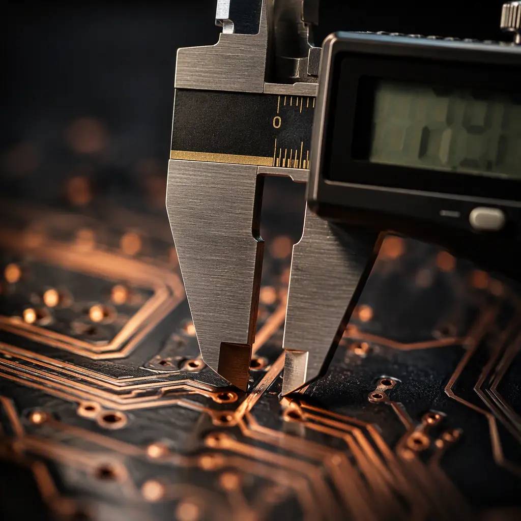
Tolerances are the contract between your design intent and the factory's process capability. A trace width callout of 0.1 mm is meaningless without the ± figure — and the difference between ±10% and ±20% can double your fabrication cost on fine-line boards. Understanding which tolerances are cheap to hold and which are expensive is one of the highest-leverage DFM skills a hardware engineer can develop.
Huaxing PCBA fabricates up to 32 layers with minimum trace and space down to 3/3 mil, and runs daily capability tracking on every tolerance class. This guide gives you the standard and tight limits we hold, the yield data behind them, and the specification strategy that keeps cost aligned with reliability. Start with our DFM tips for the yield fundamentals, then come back here for the numbers.
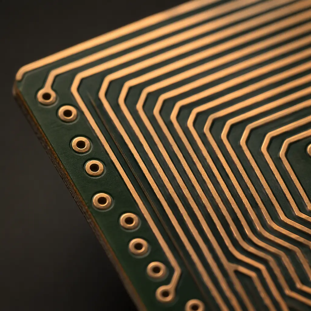
The Tolerance Family: Seven Dimensions That Matter
Not all tolerances are created equal. The seven below cover 95% of the spec errors we see on incoming fabrication drawings. Each has a standard value most factories hold routinely, and a tight value that costs extra.
| Parameter | Standard | Tight | Cost Impact of Tight |
|---|---|---|---|
| Trace width / spacing (≥0.15 mm) | ±10% | ±10% (min 0.1 mm) | None |
| Trace width / spacing (<0.15 mm) | ±20% | ±10% | Moderate |
| Drilled hole diameter | ±0.076 mm | ±0.05 mm | Moderate |
| Finished hole diameter | ±0.076 mm | ±0.05 mm | Low |
| Annular ring (external) | 0.125 mm min | 0.075 mm min | High |
| Layer-to-layer registration | ±0.075 mm | ±0.05 mm | Moderate |
| Board thickness | ±10% | ±5% | Low |
Trace Width and Etch Tolerance: Where Fine-Line Gets Real
Copper traces are produced by subtractive etching, and the etch process removes copper from the sides of the trace as well as the top — a phenomenon called etch factor or undercut. For a trace designed at 0.1 mm, the finished width can vary by ±20% depending on copper weight, etch chemistry, and panel position. That variation directly affects resistance, current capacity, and impedance.
For traces above 0.15 mm, ±10% is achievable at no cost premium. Below 0.15 mm, standard capability drifts to ±20%, and holding ±10% requires tighter process control — typically slower etch lines and more frequent coupon measurement. If your design needs precise resistance for a shunt or a sensing circuit, our trace width and current capacity guide shows how to dimension for worst-case etch rather than nominal.
Key Takeaway: Below 0.15 mm trace width, budget for ±20% etch variation. Design critical traces — shunts, sense lines, impedance-controlled nets — on worst-case width, not nominal.
Drill Tolerance: Hole Size vs Finished Hole Size
Two numbers get confused on every drawing: the drilled hole size and the finished hole size. The drilled hole is what the machine cuts; the finished hole is what remains after plating — typically 0.075–0.1 mm smaller. Mechanical drilling holds ±0.076 mm on standard diameters; laser-drilled microvias below 0.15 mm hold ±0.025 mm but are a different process entirely. See our laser vs mechanical drilling comparison for when each applies.
For press-fit connectors and interference-fit pins, hole tolerance is a functional parameter, not a cosmetic one: a ±0.05 mm shift can change press-in force by 30% or more. If your board uses press-fit terminals, specify the finished hole tolerance explicitly and ask for a hole size report on the first article. Our press-fit technology guide covers the full spec chain.
Annular Ring: The Tolerance That Kills Yield
Annular ring is the copper ring surrounding a drilled hole — the margin that keeps the barrel connected to the pad when drill and registration drift. It is the single biggest yield driver on standard boards. Standard minimum external annular ring is 0.125 mm; tight designs push to 0.075 mm. Below that, breakout risk climbs sharply and every panel becomes a lottery.
The arithmetic is unforgiving: with a ±0.075 mm drill position error and ±0.075 mm registration error, a 0.075 mm annular ring leaves effectively zero worst-case margin. That is why we recommend 0.125 mm as the floor for anything not constrained by package pitch, and why via-in-pad designs need via fill planned from day one rather than as a rework afterthought.
Layer Registration: The Multilayer Alignment Problem
Every lamination step introduces a chance for layers to shift. Standard registration between layers is ±0.075 mm; high-layer-count boards (16+ layers) with sequential lamination accumulate more risk, which is why 20+ layer stackups command a premium. Tight ±0.05 mm registration is available but pushes up the cost of tooling and inspection.
Registration tolerance interacts directly with your stackup design. Blind and buried vias — which require drilling against inner layers — demand tighter registration than through-hole-only designs. If you are planning an HDI board, read our HDI technology guide before finalizing the layer budget; the via architecture you choose determines the registration class the factory must hold.

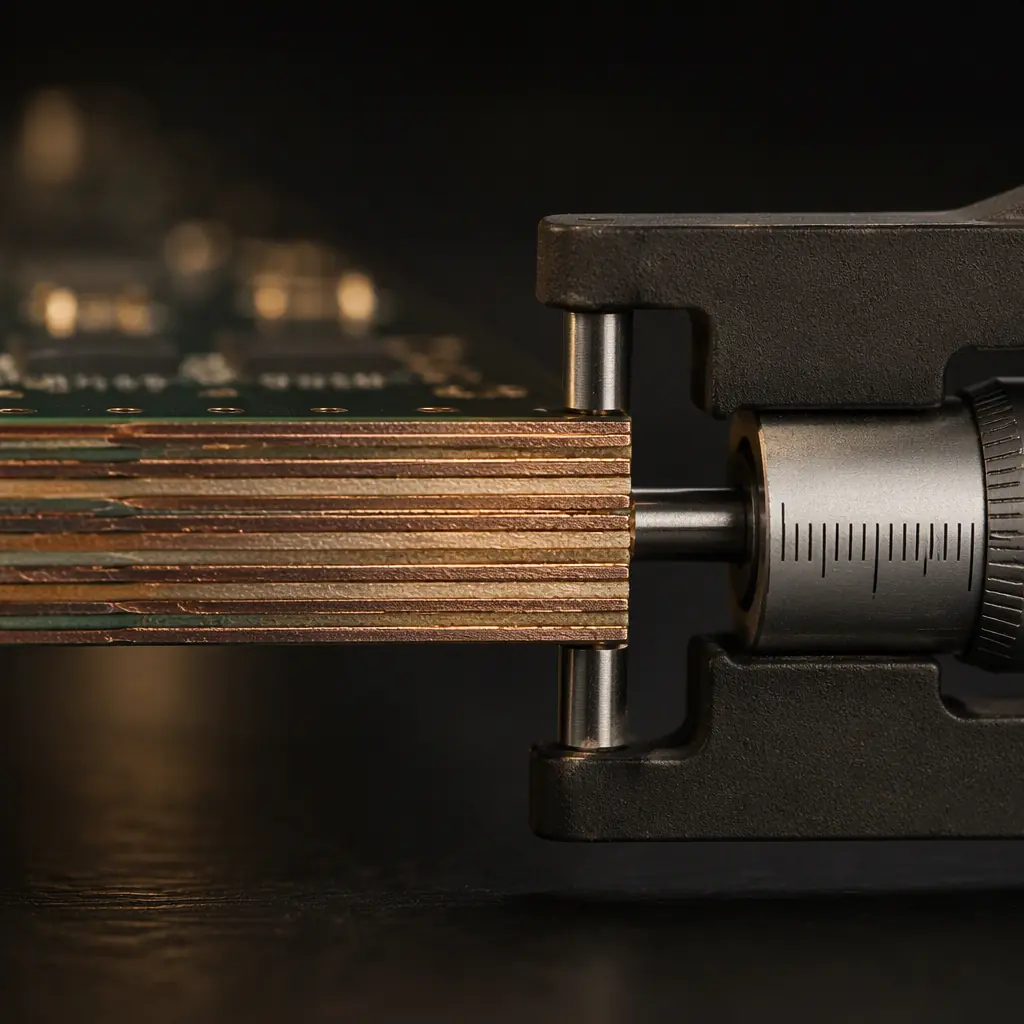
Impedance Tolerance: The One That Looks Tight but Is Negotiable
Controlled impedance boards are usually specified at ±10%, with some designs asking ±5%. Here is the manufacturing reality: impedance is a function of trace width, dielectric thickness, and copper roughness — all of which vary across the panel. Holding ±10% on a 50 ohm single-ended line is routine for a factory with impedance capability. Holding ±5% is possible but requires selective materials, tight laminate thickness control, and typically raises cost 15–25%.
The negotiation lever is location: impedance tolerance applies to the line, and coupling variations at connectors and vias are excluded. Specify impedance on the nets that matter (DDR, SerDes, RF) and leave the rest at standard tolerance. Our impedance control guide explains how to define test coupons so the report actually represents your board.
Bow and Twist: The Tolerance Nobody Puts on the Drawing
IPC-6012 allows bow and twist up to 0.75% for surface-mount boards — but a board that passes IPC bow limits can still fail your assembly process: a 1.6 mm board bowed 0.75% moves 1.2 mm at the corner, enough to shadow the solder paste stencil and cause open joints. For boards longer than 150 mm, or panels going through reflow, specify a tighter bow limit (0.5% or less) and check it at incoming inspection.
Bow is driven by copper balance, asymmetric stackups, and how the board is baked before solder mask. Our stackup design guide includes the copper-balance rules that prevent warpage at the design stage, and our warpage prevention guide covers the assembly-side controls.
Specifying Tolerances: The Three-Rule Strategy
Default to Standard Unless Function Requires Tight
Write standard tolerances on the fabrication drawing and call out tight values only on dimensions that affect fit, function, or signal integrity. Most PCB CAD tools let you set per-net or per-drawing tolerance — use per-dimension overrides rather than a global ±10% everywhere.
Separate Functional from Cosmetic
Connector footprints, press-fit holes, and impedance nets are functional — spec them tight. Everything else is cosmetic — leave it standard. A drawing that marks every dimension "critical" trains the factory to ignore the marking.
Verify on First Article, Not Just by Certificate
Request a first article inspection report with actual measurements — trace widths, hole sizes, annular ring, and impedance coupons — and compare against your drawing. Our first article inspection guide lists exactly which measurements to demand.
Key Takeaway: Tolerance strategy is a yield calculation, not a virtue signal. Standard tolerances where function allows, tight tolerances where physics demands, and first-article verification that the factory actually held what you asked for.
Summary: Turn Tolerances into a Cost Advantage
Correctly specified tolerances reduce fabrication cost, improve yield, and eliminate incoming inspection surprises. The rules are simple: hold ±10% on traces above 0.15 mm, keep annular ring at 0.125 mm unless pitch forces tighter, budget ±20% on fine-line etch, and verify with first-article measurements. For the process side of the equation, pair this with our materials guide and copper weight selection guide.
At Huaxing PCBA, we publish our capability matrix — standard and tight limits for every tolerance class — and we will review your fabrication drawing for free before you commit. Start with the DFM checklist or send your Gerbers for a tolerance audit and a quote with realistic capability callouts.
