
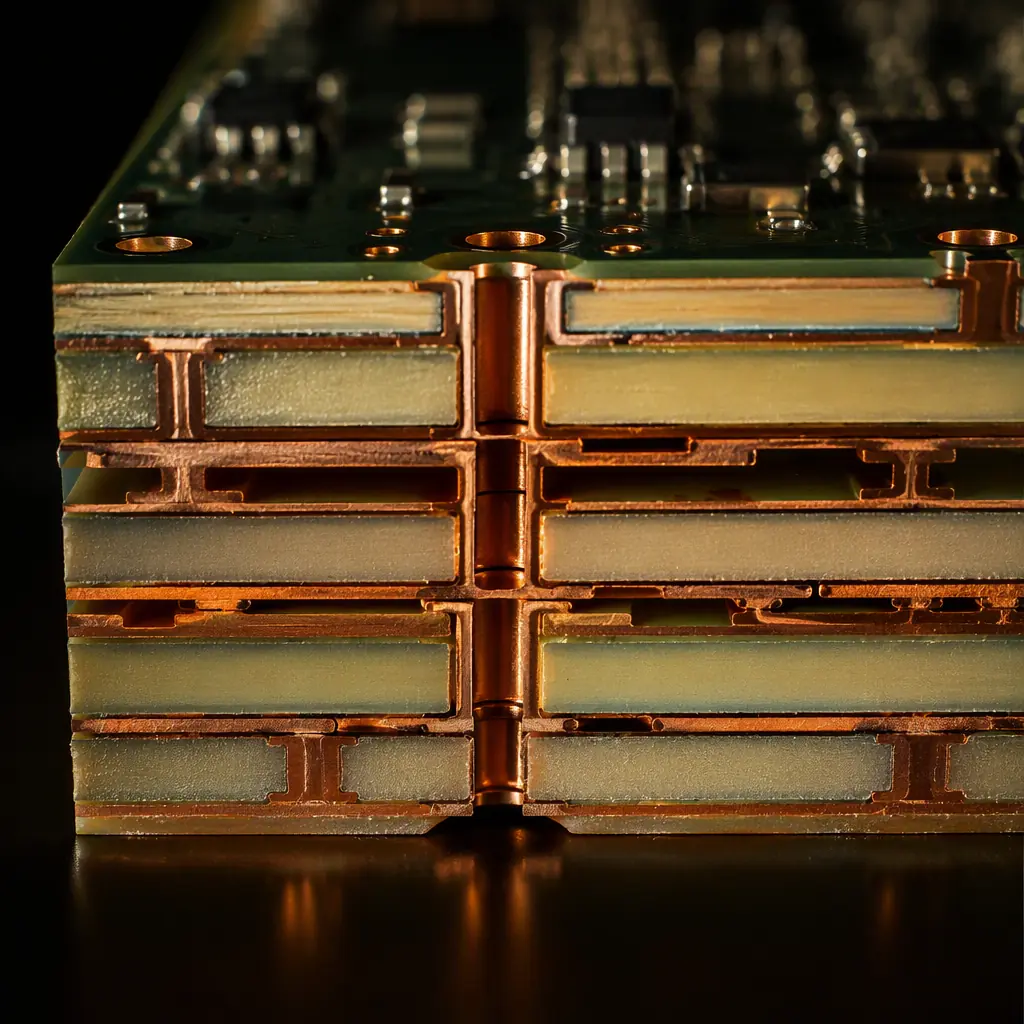
Board thickness is the most spec'd and least understood dimension on a fabrication drawing. Everyone writes "1.6 mm" because that is what the last board used, but thickness is loaded: it sets your controlled impedance by fixing the dielectric distance between reference planes, it determines whether the board is stiff enough to survive handling and connector insertion, and it either saves you from warpage or guarantees it. This guide replaces the default with a deliberate decision.
At Huaxing PCBA we fabricate boards from 0.2 mm to 6.0 mm, from 2 layers up to 32 layers, so we see the full range of what thickness needs to achieve. The principles below apply regardless of which factory builds your board.
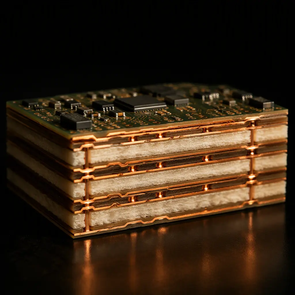
How Thickness Actually Interacts With Your Design
Thickness is not an isolated property. It interacts with four other variables, and changing it cascades through all of them:
Controlled Impedance
Single-ended impedance depends on trace width, dielectric thickness (the space between the trace and its reference plane), and the material's dielectric constant. For a given target impedance, a thinner board forces thinner dielectric spacing and narrower, more manufacturing-sensitive traces. A thicker board gives you more dielectric, so your 50 Ω trace is wider and easier to etch consistently. See our impedance control guide for the full treatment.
Stiffness and Mechanical Support
A thin 0.8 mm board flexes under a heavy connector or a force-sensing application. A 2.4 mm board holds up to a backplane guide or a high-insertion-force board-to-board connector. Pick thickness by what the board physically has to survive, not by preference.
Warpage Risk
This is the one people forget. A thin board with asymmetric copper across layers will warp in reflow. Thick boards resist warpage better, but a very thick board with heavy copper lamination can still bow if the copper distribution is unbalanced. See our warpage and reflow prevention guide and our copper weight selection guide for more detail.
Layer Count and the Stackup
Thickness is the sum of the laminates and prepregs you stack. Add layers and the board naturally gets thicker. The relationship is not optional, see our layer count selection guide and our stackup design guide to understand how the two are linked.
The Standard Values, and What Each Is For
There is a set of standard thicknesses that factories keep in inventory. Sticking to them saves cost and lead time because the laminates are already stocked. Here is the practical map:
| Thickness | Typical Use | Design Note |
|---|---|---|
| 0.4–0.6 mm | Flex/rigid-flex, smart cards | Very thin, needs rigid support or flex capability |
| 0.8–1.0 mm | Wearables, mobile, compact modules | Light, but watch stiffness and copper balance |
| 1.6 mm | General purpose, 2–8 layers | The default, best cost/performance balance |
| 2.0–2.4 mm | High-current, backplanes, industrial control | More room for heavy copper, more stiffness |
| 3.0–3.2 mm | Power electronics, high layer count | Best stiffness, heavier and pricier |

Thickness and High Current, When You Go Thick
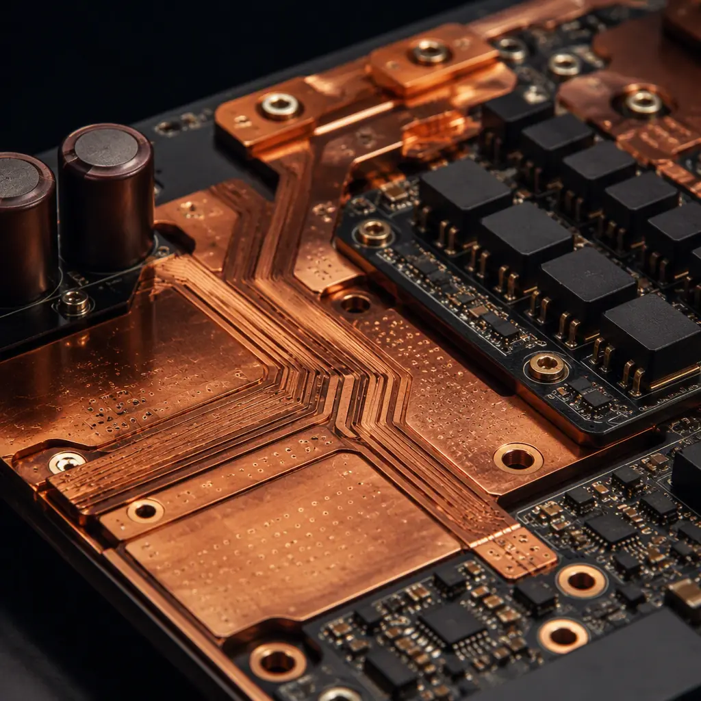
For power boards, thickness brings a second benefit beyond stiffness: room for heavy copper. A thick board can carry high current through wide, fat traces on an outer layer and thick internal planes. If your board is pushing tens of amps, you will want to think about both the copper weight and the board thickness together. See our heavy copper PCB guide and our trace width current capacity guide for the numbers.
Impedance Still Matters on Thick Boards
A 3.2 mm board with a 50 Ω single-ended trace needs a much wider trace than the same impedance on 1.6 mm. If you route high-speed signals on a thick power board, check your stackup math for the actual dielectric thickness. Our signal integrity guide and materials guide cover the material side.
Thermal Considerations
A thicker board with heavier copper conducts and spreads heat better, which matters for hot components. But it also has more thermal mass and takes longer to reach reflow temperature. Balance current, thermal, and reflow behaviour together. See our thermal management guide.
Choosing Between 0.8, 1.0 and 1.6 mm for Space-Constrained Designs
The most common real decision is not thick versus thin. It is how thin you can safely go for a compact design. Wearables, portable medical devices, handheld instruments and small IoT modules all compete for millimetres of vertical space, and the temptation is to drop straight to 0.8 mm or 0.6 mm. That saves space but costs stiffness, routing room, and assembly tolerance. Here is the practical trade-off matrix:
| Thickness | Stiffness | Layer Floor | Typical Products |
|---|---|---|---|
| 0.6 mm | Very low, needs support or flex | 2 layers | Smart cards, flex, thin display |
| 0.8 mm | Low | 2–4 layers | Wearables, sensor modules |
| 1.0 mm | Moderate | 2–6 layers | Handheld, portable medical |
| 1.6 mm | Good | 2–14+ layers | General, most electronics |
Thin Boards Need Copper-Balanced Stackups
A 0.8 mm board warps far more easily than a 1.6 mm one, and the cause is almost always asymmetric copper. If you go thin, balance the copper weight across layers, avoid a solid plane on one side and sparse routing on the other, and plan for a flatness requirement. Your fab should hold IPC-6012 Class 2 flatness, be explicit about it. See our PCB manufacturing tolerances guide for the numbers.
Connector and Component Compatibility
A 0.8 mm board is fine for a board-to-wire JST header but may not suit a press-fit backplane connector that needs a stiff board to hold up to insertion force. If you are mating into a card-edge or board-to-board connector, match the thickness to the connector's design tolerance. For press-fit, see our press-fit technology guide.
Rigid-Flex: Thickness Changes at the Boundary
In a rigid-flex design, the rigid regions and the flex regions have different thickness needs, and the transition zone is where stress concentrates. Keep the rigid area at a thickness that supports the components, and drop to the flex thickness only in the bending area. See our flex PCB design guide for the constraints.
How Thickness Affects Cost and Lead Time
Thickness is not free. Thicker boards use more material, more laminate, and often more process time. Extremely thin boards (below 0.8 mm) are also fiddly. They need careful handling and can slip in plating. Both ends of the spectrum cost more than the comfortable middle.
Stick to Stocked Values
0.8, 1.0, 1.6, 2.0, 2.4 and 3.2 mm are the values factories keep in inventory. A non-standard thickness like 1.2 mm or 2.7 mm may require special laminate ordering, adding lead time and cost. Ask your factory for their standard thickness table before committing.
Panelisation and Edge Clearance
Thickness also affects how a board panelises, how it is routed or V-scored, and how it behaves in depaneling. A very thin board is more likely to flex and crack during depaneling. See our panelization and cost optimization guide and our depaneling methods guide for the practical constraints.
Summary, Choose Thickness Deliberately
Default to 1.6 mm, deviate for a reason. Go thin for space and weight, and accept the added stiffness and warpage care that comes with it. Go thick for current, heat, and rigidity, and budget for the extra material and processing. Make the call with the trace width, copper weight, layer count and stackup beside it. Because thickness is a lever that moves all of them.
At Huaxing PCBA we build from 0.2 mm to 6.0 mm across 2–32 layers on an 88,000 m² campus, with controlled-impedance capability and IPC Class 2/3 acceptance. Send your files for a quote and our CAM team will verify your stackup and thickness before production, or talk to an engineer about the right value for your board.
