

Design for Assembly (DFA) is the practice of making component choices and layout decisions that are easy for an SMT line to build. It is distinct from DFM (design for manufacturability, which is about fabrication) and DFT (design for test). DFA targets the assembly step specifically. And it is where most of your recurring cost and rework risk actually lives.
Across our 8 SMT lines at Huaxing PCBA, we see the same DFA mistakes repeat in customer designs: exotic package sizes that slow placement, missing fiducials that break optical alignment, and test points that no fixture can reach. Fixing these at layout time costs nothing. Fixing them after production starts costs money on every single board.

Rule 1: Standardize Your Component Sizes
Every unique package size on your BOM costs placement time and feeder slots. A board with ten different passive sizes forces the line to change nozzles and re-tune placement programs. A board with two sizes, say 0402 and 0603 for passives, one QFP, one BGA, flies through the line.
The economics are concrete: a typical pick-and-place machine places a 0402 at 30,000+ placements per hour, but placement rate drops as package variety grows because of nozzle changes. Consolidating three passive sizes into one can cut assembly time per board by 10–15% with zero change in electrical performance.
Key Takeaway: Ask yourself: does this 0201 resistor really need to exist, or can it be a 0402? Every exotic package you remove makes your board faster and cheaper to build.
Rule 2: Give Components Generous Orientation Flexibility
Polarized components, diodes, capacitors, connectors, need consistent orientation for automated placement. If your footprint forces a specific rotation for most parts but one component must be rotated 180°, the placement program handles it fine, but manual inspection and rework become error-prone.
More important: keep all polarized components on one side where possible. Mixed-side placement (components on both top and bottom) is possible, our assembly process guide explains double-sided reflow, but it roughly doubles the number of process steps, and every extra pass adds cost and defect opportunity.
Rule 3: Design Footprints From the Datasheet, Not the Library
Default CAD library footprints are often built for the best case, not the real part. The result is pads that are too small for the actual package, causing tombstoning and poor solder joints. A footprint tuned to the datasheet's recommended land pattern, with correct pad size, solder mask opening, and paste aperture, assembles cleanly the first time.
This is a design-time fix with a manufacturing-time payoff. Tombstoning rework on a board with 1,000 passives costs far more than the hour it takes to verify footprint dimensions against the datasheet. Our DFM tips article covers the fabrication-side rules; footprint verification is the assembly-side twin.
Rule 4: Add Fiducials, Even on Small Boards
Fiducial marks give the placement machine's vision system a reference point. Boards without fiducials rely on edge registration, which drifts as panels expand and shrink during reflow. The result is misaligned components that fail AOI and need rework.
The standard is three fiducials, two for position, one for rotation, placed at panel corners with clear solder mask-free copper, typically 1 mm diameter. They cost nothing to add in layout and can eliminate the single largest source of placement misalignment. If your CM has to add fiducials at manufacturing time, you pay for it.
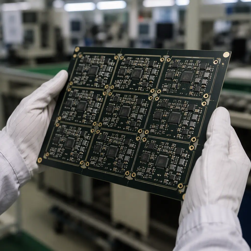
Rule 5: Panelize for the Assembly Process, Not Just Fabrication
Panelization decisions affect assembly as much as fabrication. Our panelization guide covers cost optimization; the assembly-side rules are:
Keep enough edge clearance for the conveyor
Assembly machines need a component-free edge strip (typically 3–5 mm) on the panel rails. Components placed too close to the edge get knocked off by the conveyor rails.
Use tooling holes for depaneling registration
Routing and V-scoring need registration features. Without them, depaneling stress can crack ceramic capacitors near the panel edge, a failure mode that shows up as field failures months later.
Put test points where the fixture can reach
Bed-of-nails fixtures need access from below. Components blocking the underside force expensive fixture redesigns or functional-test-only coverage. Our DFT guide has the full checklist.
Rule 6: Design for the Solder Process You'll Actually Use
Whether your board uses reflow for SMT, wave or selective for through-hole, or a mix, the design must match the process. A board that mixes fine-pitch QFPs with large through-hole connectors forces a complex process flow: often requiring a second soldering pass or hand soldering, both expensive.
Key choices that keep the process simple:
Minimize through-hole on SMT-dominant boards
Each through-hole component on an SMT board may need selective soldering or manual soldering. If through-hole is unavoidable, cluster it in one area so the selective solder machine makes one pass.
Match pad finishes to the assembly process
ENIG and OSP both assemble well, but OSP has a shorter shelf life and needs careful handling. Our surface finish guide covers the trade-offs.
Watch the thermal balance of the board
Large copper planes and heavy components heat slower than small pads, causing reflow defects. Copper balancing, the fabrication rule in our DFM guide . Is also an assembly rule: uneven heating means uneven solder joints.
Rule 7: Plan Test Access in the Layout
Test strategy is a DFA concern because it drives fixture cost and test time. A board designed without test points forces either a flying probe (slower, cost per board) or a custom functional test fixture (expensive NRE).
Three rules keep test cost down:
Put test points on a standard grid
Fixtures use standard probe spacing. Test points off-grid force custom probes that cost 3–5× more and wear faster.
Expose the points on the same side
Single-sided test access means one fixture. Double-sided access doubles fixture cost and probe count.
Make the points big enough
0.9–1.0 mm test pads are the sweet spot, small enough to save space, big enough for reliable probe contact. See our test method comparison for how this choice interacts with volume.
Rule 8: Keep Documentation Assembly-Ready
The BOM and assembly drawing are the line's instructions. Missing data, polarity markings, orientation notes, alternate part numbers, stops production or produces wrong assemblies. Our Gerber prep guide covers file readiness; the assembly side needs:
Polarity and pin-1 indicators on the assembly drawing
Explicit marks for diodes, capacitors, connectors and IC pin 1. Ambiguity here is the #1 source of wrong-part assembly.
Manufacturer part numbers, not just descriptions
"10k resistor 0402" leaves room for error. "RC0402FR-0710KL" does not. Full MPNs with alternates listed speed sourcing and prevent substitution mistakes.
Mark sensitive components
ESD-sensitive, moisture-sensitive (MSL) and temperature-sensitive parts need explicit flags so handling follows the right procedure. Our MSL guide explains the risks.
Rule 9: Budget for Rework in the Design
Every board will eventually need rework, a failed component, a test escape, a field return. Boards designed with rework in mind cost far less to repair:
Keep 1–2 mm of clearance around BGAs and QFPs
Rework tools need access to the component edges. Tight layouts make hot-air rework risky for neighbors.
Avoid conformal coating over rework-prone areas
Coating removal before rework adds time and risk. If coating is needed, mask the areas most likely to need repair. Our conformal coating guide covers masking strategy.
Specify spare test points for debug
Two or three extra exposed test points for scope probing turn a "can't diagnose" field return into a 20-minute fix.

Rule 10: Measure DFA Success With the Right Metrics
DFA isn't a one-time review, it's a feedback loop. The metrics that tell you whether your design assembles well:
| Metric | What It Measures | Healthy Range |
|---|---|---|
| First-pass yield (FPY) | Boards passing AOI + test without rework | >98% for mature designs |
| DPPM | Defects per million placed components | <100 for stable SMT |
| Rework rate | % of boards needing manual touch-up | <2% for DFA-clean boards |
| Placement cycle time | Time per board on the line | Falls 10–15% after component consolidation |
Our quality metrics guide explains how to interpret these numbers and what to demand from your CM. If your assembler reports FPY below 95%, ask for the defect Pareto. It will point straight at a DFA rule this article covers.
The Bottom Line
DFA is the highest-leverage cost reduction available to a hardware team. It costs nothing at layout time and saves money on every board ever built. The ten rules here, standardized components, datasheet-tuned footprints, fiducials, assembly-aware panelization, process-matched design, test access, clear documentation, rework-ready layout, and honest metrics, cover the majority of assembly cost and quality risk.
At Huaxing PCBA, our engineering team reviews every incoming design for assembly risk before production, free of charge. Send us your Gerbers and BOM for a DFM/DFA review and 24-hour quote . We'll flag the DFA issues in this article before they cost you money.
