
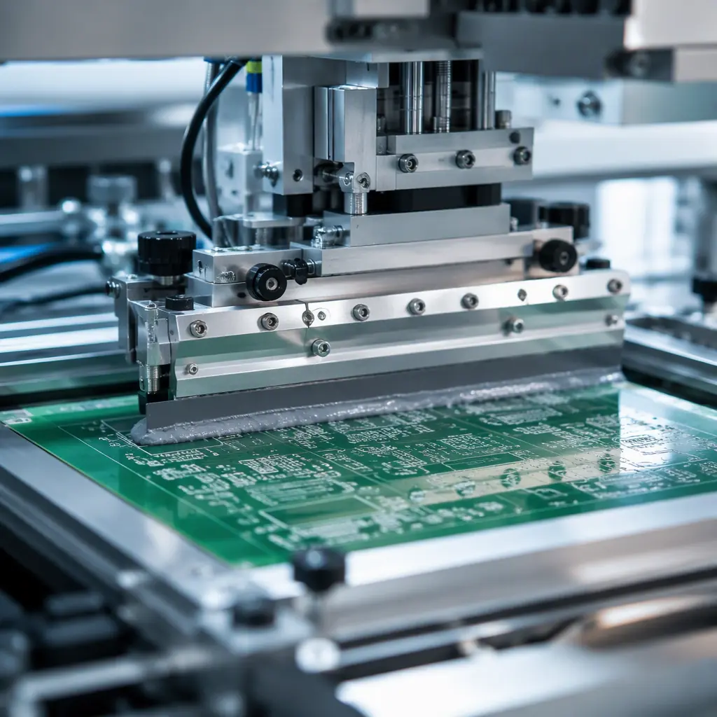
Every SMT line starts the same way: solder paste has to land on the pads before a single component is placed. For decades that meant one process, stencil printing. But piezoelectric jetting has quietly become a serious alternative for boards where a stencil is overkill. This guide breaks down the real engineering and cost differences, so you can spec the right process instead of paying for the wrong one.
At Huaxing PCBA, our SMT department runs 8 lines with both stencil printers and jet dispensing capability. We use each process where it earns its keep, and we've seen what happens when buyers specify the wrong one. This article gives you the numbers behind that decision, from deposit accuracy to per-board tooling amortization.
What "Zero Tooling" Actually Means in SMT
A stencil is a laser-cut stainless steel foil with apertures matched to your pad pattern. It costs money, takes time to produce, and is locked to one board design. "Zero tooling" means the jet dispenser needs none of that: the paste pattern is defined in software and can change between boards with no hardware swap.
The practical consequences matter more than the slogan:
No stencil lead time
A laser-cut stencil typically takes 24–72 hours to produce, and rush delivery doubles the cost. Jetting starts printing the moment the program loads. Same-day paste application is realistic, which is why it pairs naturally with quick-turn assembly.
Zero stencil NRE at any revision
Every board revision with a stencil process means a new stencil: typically $50–$300 each depending on size and frame. With jetting, a design change is a software update. For iterative prototyping, this compounds fast. See our breakdown of PCB NRE and tooling costs for the full picture.
Design flexibility without compromise
Jetting handles step-stencil scenarios, different deposit heights on the same board, without the cost and complexity of a multi-step stencil. Mixed 0201 and QFP boards are printed in one pass with per-site volume control.
Key Takeaway: "Zero tooling" is not a marketing phrase. It means zero stencil cost, zero stencil lead time, and zero stencil revision cost. The trade-off is cycle time per board, which only matters at volume.
How Solder Paste Jetting Works
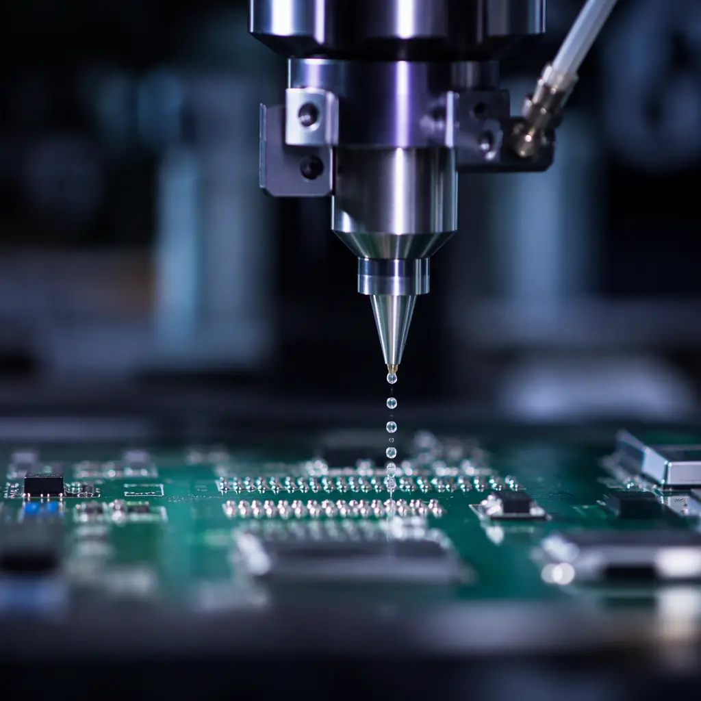
A piezoelectric jet head works like an inkjet printhead scaled up for solder paste. A ceramic element pulses thousands of times per second, forcing paste through a small nozzle as discrete droplets. The head moves across the board, placing droplets only where the program says, no apertures, no squeegee, no under-stencil wipe.
Three specifications define whether a jet process can handle your board:
| Parameter | Typical Jetting Range | What It Means for Your Board |
|---|---|---|
| Minimum deposit size | ~0.3 mm diameter dots | Fine-pitch pads down to 0201 and 0.4 mm pitch QFP |
| Deposit volume control | ±5% per dot | Tighter than stencil's ±10–15% on small apertures |
| Deposit height | Variable per site | Step-printing behavior without stencil steps |
Because the paste is applied in droplets, the final deposit is a stack of dots, slightly domed rather than the crisp brick shape a stencil produces. For almost all SMT components this is electrically and mechanically equivalent after reflow, but it matters for very fine pitch (below 0.4 mm) where paste volume control is critical. Our fine-pitch SMT assembly guide covers the 01005/0201 side of that question in detail.
Stencil Printing vs Paste Jetting: The Honest Comparison
No process wins every category. Here is the comparison table procurement and engineering teams actually use:
| Criteria | Stencil Printing | Solder Paste Jetting |
|---|---|---|
| Tooling cost (NRE) | $50–$300 per stencil | Zero |
| Setup / changeover | 5–15 min per board change | <1 min (software only) |
| Print cycle time | ~10–30 s per board | 1–5 min per board (density dependent) |
| Deposit accuracy | ±10–15% volume (small apertures) | ±5% per dot |
| Step printing (mixed heights) | Multi-step stencils, expensive | Native, no extra cost |
| Stencil cleaning / upkeep | Under-stencil wipe, periodic chemistry | No stencil to clean |
| Best volume range | ~1,000+ boards | 1–1,000 boards |
Two facts deserve emphasis. First, stencil printing's speed advantage is enormous. A printer does a board in seconds while a jet head takes minutes. Second, jetting's accuracy advantage is real but narrow: it shows up on small apertures where stencil transfer efficiency drops below 80%. On large pads both processes are more than adequate.
Where the Costs Actually Break Even
The decision is a volume math problem. Stencil NRE is fixed; jetting has no NRE but a higher per-board time cost. Here is a realistic model for a 10 cm × 10 cm board with ~300 components:
| Volume | Stencil Cost/Board | Jetting Cost/Board | Winner |
|---|---|---|---|
| 5 boards (prototype) | $60+ NRE spread over 5 | No NRE, slower cycle | Jetting |
| 50 boards (pilot) | NRE still significant | No NRE, manageable time | Jetting |
| 500 boards | NRE amortized thin | Cycle time starts to bite | Near break-even |
| 5,000+ boards | Full speed, minimal cost | Time cost dominates | Stencil |
The crossover sits roughly between 300 and 1,000 boards depending on board density, paste type, and stencil price. Below that, jetting almost always wins on total cost. Which is exactly why it is the default recommendation for prototype and low-volume builds. For a deeper look at how volume reshapes pricing, see our PCB cost drivers article.
Procurement Tip: When you request a quote, ask the CM which process they plan for your quantity, and what the stencil NRE is. A quote that buries a $200 stencil in the prototype price hides the fact that jetting would have been free.
Quality Control: SPI Numbers for Jetted Deposits
Jetted paste is inspected exactly like stencil-printed paste, with a solder paste inspection (SPI) machine using structured light to measure height, area and volume of every deposit. The acceptance criteria from our inspection methods guide apply identically: volume within ±15% of target, no bridging, no missing deposits.
In practice, jetted deposits show two quality characteristics worth knowing:
Lower variance on small apertures
Because each dot is metered by the piezoelectric pulse, 0201 and 0.4 mm pitch deposits hold ±5% volume consistency run to run, better than the ±10–15% typical of stencil transfer on those sizes.
Bridging risk is managed by droplet spacing
The program controls droplet pitch, so bridges between adjacent pads are preventable in software. Stencil bridges are a squeegee-pressure problem fixed by process tuning. Both are caught at SPI before reflow. The key is that the SPI step exists at all.
When Stencils Still Win, and Why That's Fine
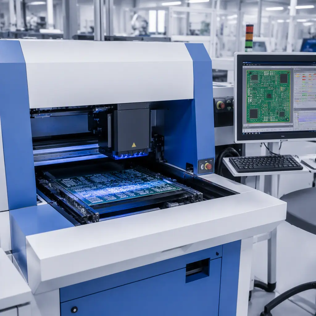
At volume, stencil printing has no rival. A printer cycles in seconds, a stencil costs pennies per board once amortized, and the process is proven over decades. If your project is headed to 5,000+ boards, stencil is the right call and jetting is a prototype-only detour.
The mistake to avoid is treating them as either/or for the whole product lifecycle. The smart pattern is:
Prototype and pilot runs, jetting
Fast, zero NRE, revision-tolerant. Perfect for prototype vs production transitions where the design is still moving.
Production, stencil
Once the design freezes and volume justifies it, cut a stencil and let the printer run at full speed. The stencil NRE is recovered in the first production lot.
Special cases, jetting in production
Mixed-height boards, panels with multiple designs, and boards with components added late in the process (selective jetting after reflow) are cases where jetting earns its keep even at moderate volume.
How to Spec Your Board for Either Process
Good news: the design rules are nearly identical for both processes. Pad size, pitch, and solder mask openings follow the same stencil design guide logic. Two things deserve attention if you think jetting will be involved:
Keep solder mask openings generous
Jetted deposits need clean, well-defined mask openings to wet properly. Tented or poorly defined openings cause the same problems as they do with stencils, uneven deposits and solder balls.
Ask about paste type compatibility
Most standard no-clean pastes jet fine, but some high-viscosity or high-silver alloys (like those in our solder paste selection guide) may need a jetting-optimized formulation. Confirm with your CM before the design freezes.
And if you're moving through the assembly flow, our PCB assembly process guide shows where printing sits in the full line, from paste to AOI to functional test.
Making the Call
Ask three questions and the answer is usually obvious:
What's the quantity?
Under ~500 boards, jetting's zero-NRE advantage usually wins the cost comparison.
Is the design still changing?
Every revision costs a new stencil. If you're iterating, jet until the design freezes.
Does the board need mixed deposit heights?
That's jetting territory, multi-step stencils are expensive and slow to produce.
At Huaxing PCBA, we run both processes across our 8 SMT lines and quote the one that fits your volume and revision cadence, not the one that pads the invoice. Send us your Gerbers for a free DFM review and 24-hour quote, and we'll tell you which paste process your board should use, and why.
