
"Coating coverage is verified by visual inspection" is the most common sentence in a conformal coating purchase order and the least testable. It does not say who inspects, under what light, against what criterion, at what magnification, or what a pass looks like. Two suppliers can both comply with that sentence while one ships boards with a bare conductor at a connector edge and the other does not, because the sentence never defined what had to be coated in the first place.
The fix is procedural, not technological. Define the zones, pick a detection method that can see into those zones, and write a criterion that produces a record. A UV tracer and a 365 nm lamp are the standard tools for the middle step, but they only work once the first and third steps exist. This guide covers all three, including the one thing UV fluorescence will not tell you, which is how thick the film is.
Define the Zone Before You Define the Test
Coverage is only meaningful relative to a map. A board is not supposed to be coated uniformly; it is supposed to be coated where the design needs protection and left bare where coating would do harm. Connectors, test points, press-fit pins, optical windows, thermal pads, board-to-board mating surfaces and anything requiring rework access all need to stay clear. The area that must be coated is therefore a shape with holes in it, not a rectangle, and no inspection method can verify a shape that was never drawn.
In practice three tiers cover almost every product, and naming them in the drawing removes most of the ambiguity that ends up in a rejection report.
| Zone tier | Definition | Acceptance | Typical content |
|---|---|---|---|
| Keep-in (Tier 1) | Coating required, coverage is functional | 100% coverage, no exposed conductor, thickness on target | Fine-pitch devices, high-impedance nodes, exposed traces, via fields |
| Conditional (Tier 2) | Coating desirable but not functional | Coating present, minor gaps accepted with documentation | Ground planes, large SMD bodies, mechanical areas |
| Keep-out (Tier 3) | Coating prohibited | Zero coating, verified by inspection | Connectors, test pads, press-fit pins, thermal interfaces, optics |
The tiers do the work that a single "coverage" percentage cannot. A board with 92% total coverage might be perfect, because the missing 8% is all Tier 3. The same board might be a total loss, because the 8% that is missing happens to be the fine-pitch area. Total area coverage is a metric that sounds quantitative and carries almost no information.
Tier 1 boundaries should follow the electrical reason, not the mechanical layout. A high-impedance node needs coating out to the point where the leakage path is broken by a keep-out or by distance, which is usually a few millimetres beyond the component body and not the component outline. Drawing the boundary at the component silkscreen is the most common reason a coverage inspection passes and the assembly still fails an insulation resistance test. The relationship between coating boundaries and clearance distances is covered in our guide to creepage and clearance on high-voltage boards.
Four Ways to Verify Coverage
The methods differ in what they can see, how long they take, and whether they leave a record. Choosing between them is a decision about escape cost against inspection cost, not a question of which is best in the abstract.
| Method | What it proves | Time per board | What it misses | Record produced |
|---|---|---|---|---|
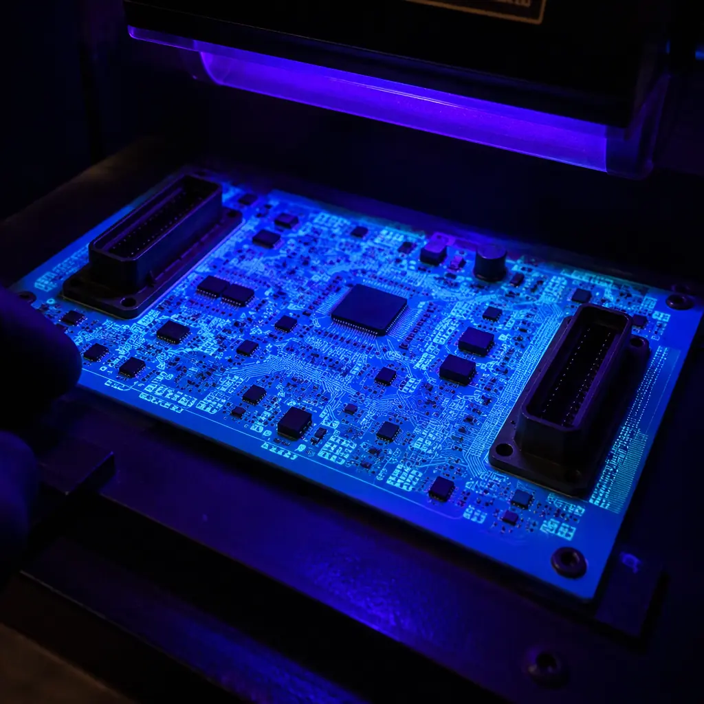
| UV tracer plus handheld lamp, visual | Presence or absence of film, gross gaps, mask leakage into keep-out | 20-60 s | Thin spots, thickness, gaps under components | Operator signature only |
| UV tracer plus fixed imaging station | Presence, area coverage against a stored zone map, repeatable between operators | 30-90 s | Thickness; anything under a shadowed component | Image with pass or fail per zone |
| Dye penetrant | Porosity and pinholes through the film | Minutes to hours | Coverage of areas the dye cannot reach; destructive on many assemblies | Photo of dye tracks |
| Destructive cross-section | True thickness at a specific point, conformity over edges and steps | Hours, sample-based | Anything outside the section plane; nothing about area coverage | Micrograph with measurements |
The imaging station is the method most assembly houses have adopted in the last few years, because it converts an operator judgement into a comparison against a reference image. Its weakness is that the reference image is itself a judgement: a board with a fisheye at the reference build becomes the standard that every subsequent board is measured against. It is worth asking who approved the reference board and when it was last re-qualified.
Dye penetrant and cross-section answer different questions and are not substitutes for area coverage. Dye finds pinholes the eye cannot see, and cross-section finds thin film at a step the eye cannot measure, but neither can tell you whether a whole zone was missed. A coverage programme that relies only on cross-sections is sampling thickness and assuming coverage, which is how a systematic gap survives a full inspection regime.
The Fluorescence Trap: Bright Is Not Thick
This is the single most important limitation to put in a purchase order, because it is the basis of a claim that sounds rigorous and is not. UV tracer fluorescence is a presence indicator. The tracer is formulated at a concentration in the coating, usually around 0.5 to 2% by weight depending on the supplier, and it fluoresces when excited by light near 365 nm. How brightly it fluoresces depends on tracer concentration, film thickness, lamp intensity, viewing angle and the observer's eye. It does not give a thickness reading, and it cannot be calibrated to one without a separate measurement.
Two consequences follow. First, a board that glows uniformly can have a film at 30 micrometres in one area and 80 in another, and the difference will not be visible. Second, and more dangerous, a board with a very thin film can look bright under a strong lamp while a board at correct thickness looks dull under a weak one. The inspection therefore proves something real, which is that the tracer is present at a location, and nothing at all about the protective function, which depends on thickness and continuity.
The correct division of labour is straightforward: UV verifies presence and zone compliance, and thickness is measured by eddy current on non-metallic substrates, by magnetic induction over steel, or by cross-section, as described in our guide to conformal coating thickness control. A supplier that presents UV photographs as thickness evidence is either misunderstanding the method or hoping the buyer will.
There is one further trap in the tracer itself. Tracer concentration drifts in an open coating bath as solvent evaporates, so a batch sprayed late in a shift can carry a higher tracer concentration and glow brighter for a given film. The fluorescence therefore varies with process time as well as with thickness, which makes any attempt to read brightness as a proxy for film build actively misleading. Tracer concentration should be checked at the same interval as viscosity.
What a Coverage Gap Actually Costs
A gap is only a defect if it enables a failure. The four mechanisms below are the ones that justify Tier 1 designation, and knowing which one applies to a particular zone is what turns a coverage map from paperwork into an engineering decision.
- Surface insulation resistance loss. A bare area between two conductors at different potentials, with flux residue or adsorbed moisture on it, provides a leakage path. The resistance falls by orders of magnitude as humidity rises, and a node at 1012 ohms in dry air can drop below the circuit's threshold at 85% relative humidity. This is the mechanism that makes coatings necessary on high-impedance analogue circuits, and it operates over the whole gap, not just at its centre.
- Electrochemical migration. With a bias voltage, adsorbed water and ionic contamination, metal dissolves from the anode and plates back as a dendrite toward the cathode. Dendrites grow fastest in the 40-80 micrometre gap range and reach a short in hours to weeks depending on bias and humidity. A gap in coating over a fine-pitch row is therefore not a cosmetic issue; it is a defined location for dendrite initiation.
- Corrosion of exposed copper and finish. Bare copper or a thin immersion finish in a condensing environment oxidises and eventually loses solderability and conductivity. On a board that will be reworked in the field, this also destroys reworkability.
- Whisker and debris bridging. In high-reliability assemblies, a gap allows conductive debris or a tin whisker to bridge without the physical barrier the coating provides. This is why Class 3 and space programmes specify coverage as a barrier requirement rather than a cosmetic one.
The gap that matters is not the one with the largest area. It is the one that sits across a voltage difference on a contaminated surface, which is usually a few millimetres wide and located at the boundary between a coated zone and a keep-out, exactly where masking removed the film. That is the area a coverage map should be built around, and the area a visual inspection under a lamp is most likely to pass without noticing.
Inspection Economics: When 100% UV Inspection Pays
Full UV inspection of every board sounds like the rigorous choice and is sometimes an expensive way to find a defect that cannot occur. The arithmetic is simple enough to do before the order is placed: inspection time per board, multiplied by volume, compared with the escape cost multiplied by the expected escape rate without inspection.
| Monthly volume | 30 s per board | 60 s per board | Extra inspector hours |
|---|---|---|---|
| 500 | 4.2 h | 8.3 h | 4.1 h |
| 2,000 | 16.7 h | 33.3 h | 16.6 h |
| 10,000 | 83 h | 167 h | 84 h |
| 50,000 | 417 h | 833 h | 416 h |
At 50,000 boards a month the difference between a 30-second and a 60-second check is a quarter of a full-time inspector, which is real money and also the point at which an automated imaging station pays for itself within a few months. Below about 2,000 boards a month, the inspection cost is small in absolute terms and the decision should be driven purely by escape cost.
Escape cost, in turn, is driven by where the product goes. A consumer device that fails in the field costs a replacement and a support ticket. A medical or automotive assembly that fails costs a warranty claim, a field action and a quality record. An assembly in a sealed enclosure that cannot be opened without destroying it costs the whole assembly plus the labour that went into it. The higher that number, the more of the board it makes sense to inspect, and the more it makes sense to buy the imaging station rather than to argue about seconds.
Where full inspection does not pay, sampling does not automatically follow. A sample inspection of coated boards is weak protection because coating defects cluster: a spray parameter that drifted affects a whole shift, and a lot sampled at the start of the run is exactly the wrong lot to sample. Where the process is qualified and SPC-controlled, a periodic audit against the zone map is reasonable. Where it is not, sampling gives false confidence at low cost, which is the worst of both.
PO Wording That Is Actually Testable
Six clauses convert everything above into something a supplier can be held to and a buyer can audit remotely. Each one is short enough to paste into a purchase order.
- Zone map as a drawing, revision-controlled, with Tier 1, 2 and 3 areas marked and dimensions given for Tier 1 boundaries. A verbal zone definition is not a requirement.
- Inspection method named per tier: for example, fixed-station UV imaging for Tier 1, visual under 365 nm lamp for Tier 2, visual under white light for Tier 3.
- Acceptance criterion per tier, stated as a result rather than an intention: no exposed conductor in Tier 1, no tracer fluorescence in Tier 3 above a stated area, documentation of any gap in Tier 2.
- Tracer specification, including that the coating contains a UV tracer at the supplier's specified concentration, and the inspection lamp wavelength (365 nm typical) and distance.
- Records that ship with the lot: the inspection images or the named inspection record, referenced to lot and date, retained for a stated period.
- Thickness verification stated separately, by a method that can measure thickness, with sample size and locations per lot. This clause exists to make clear that the UV step is not being used as thickness evidence.
The fifth clause is where remote supply chains get their leverage. An image set per lot is auditable from another continent without a site visit, and a supplier that knows the images will be reviewed tends to catch its own spray drift. The same logic applies to the other inspection stages: what cannot be reviewed remotely cannot be managed remotely, which is the theme of our guide to pre-shipment inspection.
One clause worth adding for assemblies with tight geometry: specify the maximum acceptable gap between the coating edge and a Tier 1 component body, in millimetres. Without a number, the gap is whatever the process produced, and the discussion happens after the fact with the boards already built.
Frequently Asked Questions
Do all conformal coatings contain a UV tracer? No. Acrylic and urethane coatings are commonly available with tracer, and parylene is generally inspected without one because the vacuum deposition process is inherently conformal and coverage is controlled by the process rather than by a spray pattern. Where a coating has no tracer, presence verification relies on gloss and edge inspection under white light, which is weaker and should be reflected in the acceptance risk.
Can UV inspection find a gap under a component? Generally not. The film under a large SMD body is in a shadow, and the excitation light does not reach it. Coverage under low-clearance components should be addressed by design, with a gap or a flow path, rather than by inspection.
How often should the reference board be renewed? Whenever the process, material or drawing changes, and on a fixed interval otherwise, for example annually. A reference board that has faded under UV exposure drifts the criterion without anyone deciding to change it.
Is 100% coverage ever the right requirement? Only for a board with no keep-out areas at all, which is rare. The correct requirement is 100% of Tier 1, and any drawing that says "100% coverage" without a zone map creates a conflict with the connectors it also requires to stay bare.
What about boards that fail the UV check? A gap in Tier 1 is a touch-up or a recoat, and the decision follows the same logic as any coating defect: identify the cause before deciding, because a systematic gap will reproduce. The defect tree is in our guide to conformal coating defects, causes and fixes.
Does the tracer affect the coating's electrical properties? At the concentrations used, typically 0.5 to 2% by weight, the effect on dielectric strength and surface insulation resistance is negligible and the coating's datasheet figures already include it. A tracer added by an assembly house to a coating not formulated for it is a different question and should be qualified, which is a reason to buy tracer-grade material rather than to add tracer in-house.