

Solder mask is the thin polymer layer that covers everything on a PCB except the pads, vias and test points that must be exposed. Buyers specify it as a colour or a finish and rarely go further. That is a mistake, because solder mask is a functional coating with a measurable thickness, an adhesion requirement and a registration tolerance — and every one of those three can be written into a purchase order and inspected on the delivered board.
When thickness is wrong, the failure appears much later. Mask that is too thin loses dielectric strength and protection; mask that is too thick can sit above the pad surface and interfere with paste release, or leave residue that kills solderability. When registration drifts, mask creeps onto pads or leaves dams too narrow to survive reflow. All of it is preventable, and all of it starts with replacing "good solder mask" with a specification that names the class, the thickness band and the measurement method.
This guide covers the measurable side of solder mask: what the IPC-SM-840 classes actually mean, the thickness bands that correspond to them, how registration is defined and toleranced, how each property is measured, and which downstream defects thin, thick or mis-registered mask causes. If you are still choosing the mask chemistry rather than qualifying it, start with our overview of PCB solder mask types, which covers LPI versus dry film versus UV-curable inks. This article picks up where that one stops: once the material is chosen, the thickness and registration become the levers you control.
At Huaxing PCBA we fabricate with LPI solder mask as standard across 8 SMT lines under IATF 16949 and ISO 9001, with mask thickness and registration tolerances confirmed against IPC-SM-840 at incoming inspection rather than assumed from the process sheet. The property set is documented per programme because solderability complaints later in the build almost always trace back to a mask parameter that was never pinned down.
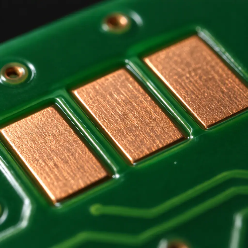
What "Thickness" Means on a Solder Mask
The first obstacle to specifying mask thickness is that it is not a single number. Solder mask is applied as a liquid or film and flows over an uneven surface — bare laminate, raised copper traces, pad edges — so its cured thickness varies depending on what is underneath. A specification that says "25 µm" without saying where is meaningless, because the same coating can measure very differently over bare laminate and over a copper trace.
Over laminate. This is the reference thickness in most discussions: the cured mask over bare base material, where there is no copper beneath. It is the thinnest measurement in most spots and is used to confirm the coating was actually applied at the intended build.
Over a trace. Where mask covers a copper trace, the coating sits on top of the raised conductor, so the height from the laminate surface includes the copper thickness. What matters for electrical function is the *dielectric thickness above the copper*, not the total height. A mask that measures generously "thick" may still be thin above the trace if the reading was taken at the wrong reference point.
Over the pad edge. The critical zone is where the mask transitions onto the pad — the dam and the mask-defined opening edge. Mask here must be thick enough to form a continuous dam but thin enough not to overhang the pad surface. This region is where most solderability problems originate, and it is the region inspection tends to skip.
Key Takeaway: "Solder mask thickness" is a family of measurements, not one number. Always state the reference surface — over laminate, over copper, or above the pad — because a single figure without a reference point cannot be inspected or enforced.
The IPC-SM-840 Class Table
IPC-SM-840, the standard for qualification and performance of permanent solder mask, separates mask into classes by end-use reliability requirement, in the same spirit as IPC Class 2 and Class 3 for the board itself. The class you specify sets how much inspection evidence and how tight a thickness band you should expect.
Class T (general/standard). Standard thickness of cured mask above the conductor in the range of roughly 0.8 mil to 1.2 mil (about 20 µm to 30 µm). This is the common commercial band and covers the majority of industrial and consumer builds.
Class H (high reliability). Stricter requirements on thickness consistency, adhesion and dielectric breakdown — applied where the mask is part of the reliability argument, such as automotive, medical and high-voltage assemblies. Class H asks for tighter process control and more complete documentation, not necessarily a radically different nominal thickness.
The practical consequence: if a supplier quotes "Class H solder mask" but cannot show a thickness distribution or an adhesion test record, the class claim is a label, not a property. Asking for the evidence is what turns the class into something you can rely on. Our PCB certifications and compliance guide covers how coating and mask claims sit alongside the certificates you collect from a fabricator.
Registration Tolerance: Keeping Mask Off the Pads
Registration is how well the mask artwork lines up with the copper artwork underneath. Every board has some misalignment, because the mask is exposed through a separate imaging step and the panel moves and shrinks through lamination and cure. The question is how much is allowed.
Mask registration is normally controlled relative to pad geometry. Where the mask openings are defined photolithographically, the tolerance is usually expressed as the allowed positional shift of the mask opening relative to the pad centre, plus the resulting minimum width of the mask dam between adjacent pads. Two numbers matter:
Pad opening clearance. The mask opening must be positioned so the exposed pad area is not reduced below what the assembly process needs. If the opening shifts, one side of the pad gains mask overhang while the other side exposes the adjacent laminate. Both are defects: overhang interferes with paste release, exposed laminate beside a pad is a potential contamination and adhesion site.
Dam width. The mask strip between two adjacent pads must stay wide enough to prevent solder bridging. On fine-pitch parts the dam between pads is already only a fraction of the pad pitch, and a registration shift in the wrong direction can narrow it to the point where it lifts or where solder bridges at reflow. This interaction with pad definition is covered in detail in our SMD versus NSMD pad design guide, where mask-defined and copper-defined pads behave differently under the same registration error.
A workable registration requirement names the reference (mask opening relative to pad), the allowed positional tolerance, and the minimum dam width after worst-case shift. Defects that overhang a pad edge during assembly are frequently mistaken for a coating problem when the real cause is registration — which is one route into black pad syndrome on ENIG boards, where mask and pad-edge chemistry interact badly.
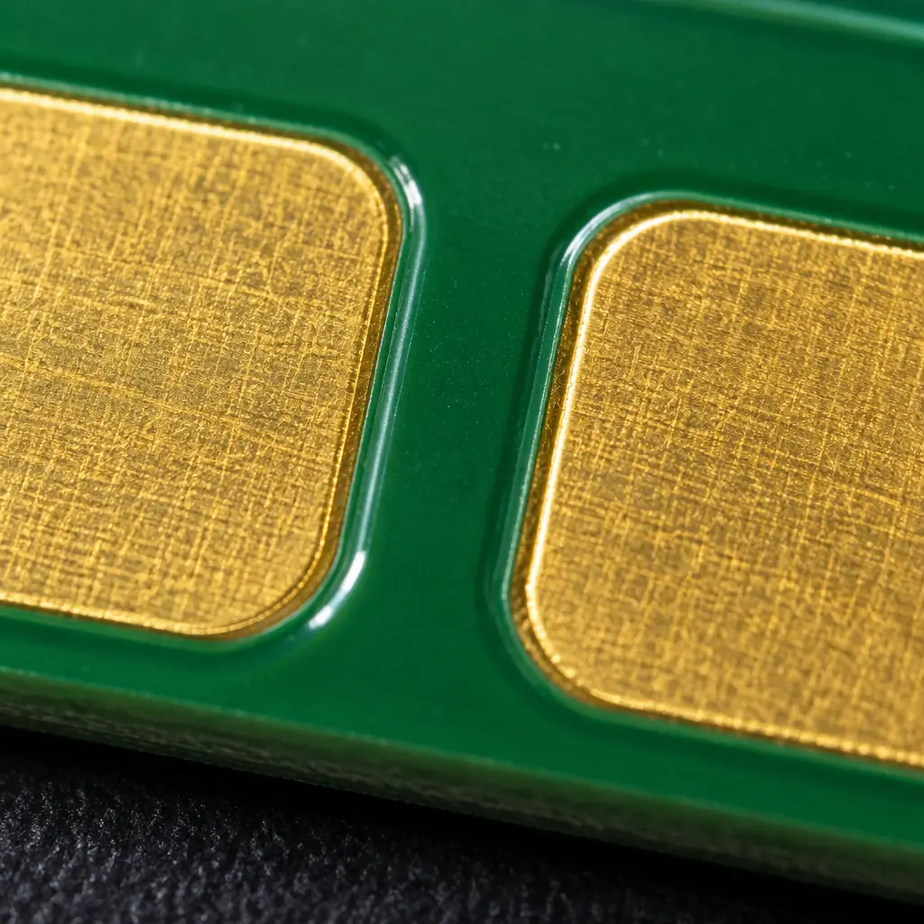
How Thickness Is Actually Measured
Thickness can be measured several ways, and they do not always agree. Knowing the method behind a reported figure tells you how much to trust it.
Cross-section. A coupon or sample board is potted, ground and polished, then the mask layer is measured under a microscope. This is the reference method: it shows the actual cured thickness over laminate, over copper and at the pad edge in one view, and it is the method a disagreement is settled with. It is destructive and slow, so it is done on coupons and first articles rather than every panel. Our guide to reading a cross-section report explains what to look for in the micrograph.
Optical and non-contact gauges. Bench instruments measure coating thickness above a reference surface without cutting the board, useful for process monitoring and for non-destructive spot checks. Their reading depends on setting the correct reference, which is exactly the reference ambiguity discussed earlier — a gauge measuring from the laminate surface over a trace reports copper plus mask, not mask alone.
UV and fluorescence methods. Some cure-state and thickness checks rely on the mask's response to UV, which can confirm cure as well as coating presence. These are process tools, not acceptance measurements.
The practical rule: accept cross-section as the reference, treat bench-gauge numbers as process indicators, and always require that a reported figure states its reference surface and method. A supplier that reports one number for "mask thickness" without qualification has not measured the property you care about.
Adhesion and Solvent Resistance
Thickness is only half of the mask specification. A mask of correct thickness that has not properly adhered to the board or cured will fail in service regardless of how it measures. IPC-SM-840 addresses both with defined test methods.
Adhesion (tape test). A defined tape is applied to a scribed or prepared mask surface and peeled under controlled conditions; the standard prescribes the tape, the cross-hatch pattern and the pass criterion. Mask that lifts with the tape has failed adhesion, and the usual causes are under-cure, contamination on the laminate before coating, or insufficient surface preparation. This test is quick and is why first-article and periodic coupons should include it.
Solvent and chemical resistance. The cured mask is exposed to flux, cleaning chemistry and, in some flows, solvent washing. The standard defines resistance tests against specified chemistries. A mask that softens or blisters under cleaning chemistry can shed residue onto pads later in the assembly, a failure that presents as a mysterious solderability loss. The interaction between cleaning chemistry and coating is why our comparison of no-clean versus water-wash flux is relevant to mask selection as well as to flux choice.
Procurement tip: Ask for the adhesion and solvent-resistance test records alongside the thickness data. Mask thickness without cure and adhesion evidence is a partial specification, and it is the partial spec that produces the late-stage solderability complaint.
What Thin, Thick and Mis-Registered Mask Cause Later
The reason to specify these properties carefully is that the failure modes they prevent all appear somewhere other than the mask station.
Mask too thin. Reduced dielectric strength, weaker protection against electrochemical migration and contamination, and lower resistance to handling damage. In high-voltage or high-humidity applications a thin mask is a reliability risk rather than a cosmetic one.
Mask too thick or overhanging the pad. The mask edge sits above the pad plane, so it can interfere with stencil seating and paste release on fine-pitch apertures, and it can shed particulate onto the pad. This is one contributor to the paste release problems discussed in stencil aperture design and paste release.
Mask residue on pads. Incomplete development or a mask formulation that does not cleanly clear the pad leaves a thin organic film on the exposed copper. It is often invisible but destroys solderability, and it is a classic cause of a board that looks perfect and will not wet. Where a finish is involved, the residue can also contaminate the surface finish chemistry, which is part of the mechanism behind black pad on ENIG.
Dam lifting after reflow. A dam that is too narrow or under-adhered lifts at reflow temperature, exposing the underlying copper and creating a site for bridging or corrosion. The cause is registration or adhesion, but the failure is observed as a solder defect.
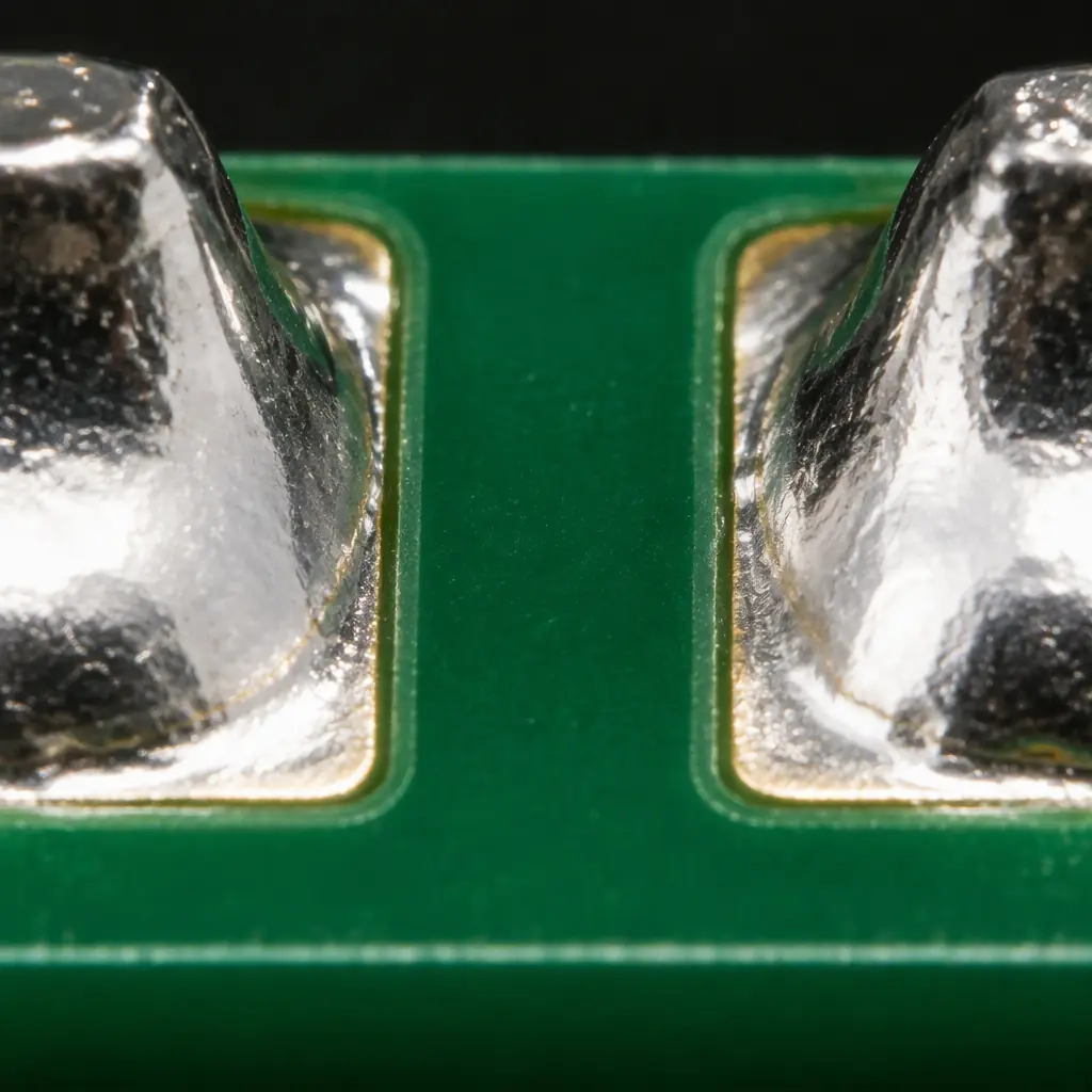
Solder Mask Requirement Checklist for the RFQ
Solder mask is a specification, and like any specification it is only enforceable if it is written down with its measurement conditions. The list below is what turns a colour and a class label into a requirement a supplier can be held to.
Name the class and the standard
State IPC-SM-840 and the class — Class T for standard commercial, Class H where the mask is part of the reliability argument. A class without the standard named invites a different interpretation.
State the thickness band and its reference surface
Give the nominal thickness and tolerance, and say whether it is measured over laminate, over conductor, or above the pad. This one clarification removes most of the ambiguity that makes mask thickness unenforceable.
State the registration tolerance and minimum dam width
Give the allowed positional shift of the mask opening relative to the pad, and the minimum dam width that must survive worst-case misregistration. Fine-pitch designs should tighten this. Coordinate it with your pad definition using our SMD vs NSMD guide.
Require adhesion and solvent-resistance evidence
Ask for tape-test adhesion results and chemistry-resistance records per the standard, on first article and on periodic coupons. This is what distinguishes a cured, adhered mask from one that merely measures to thickness. See PCB incoming quality inspection for where these records are checked against the delivered board.
State the pad-clearing requirement
Require that pads are free of mask residue and that the opening clears the pad by an agreed margin. This is the requirement that prevents the invisible organic film behind so many late solderability failures.
Put the mask spec in the same package as the rest of the build spec
Mask requirements belong with your surface finish, tolerance and inspection clauses so they are reviewed together, not as an afterthought. Our PCB specification and RFQ guide shows how the clauses are assembled into one document.
Summary: Mask as a Number, Not an Adjective
Solder mask protects the board, defines where solder can land and contributes to the reliability argument in demanding applications — but only when it is specified as a measurable property rather than a colour and a claim. Thickness with a named reference surface, a class from IPC-SM-840, a registration tolerance with a minimum dam width, and adhesion and solvent-resistance evidence together form a specification that can be inspected on the delivered panel. The failures that follow from getting it wrong — marginal solderability, dam lifting, residue on pads — almost never appear at the mask station; they surface later as solder defects and reliability doubts, which is exactly why the spec belongs in the purchase order up front.
At Huaxing PCBA we fabricate with LPI solder mask under IPC-SM-840 control as standard across 8 SMT lines under IATF 16949 and ISO 9001, and we document mask thickness, registration and adhesion evidence per programme rather than treating the mask as a cosmetic layer. If mask performance is part of your reliability case, tell us the class and the environment and we will build the specification around it. Send your Gerber and BOM and we will confirm the mask parameters for your build and return a quote inside 24 hours, or talk to our engineering team about a solderability concern you are tracing.
