
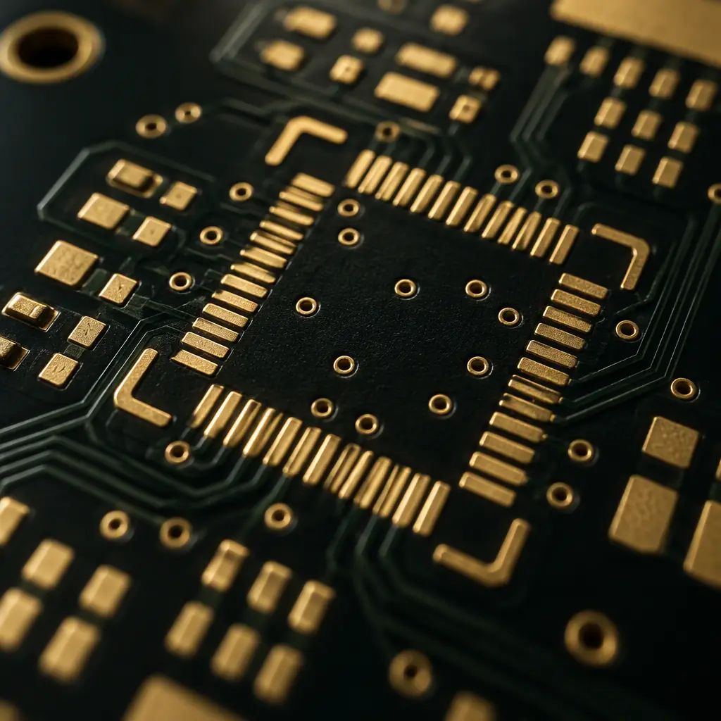
Black pad syndrome is the one defect in PCB surface finishing that buyers remember after it bites them, because it is invisible at incoming inspection, absent at assembly, and then suddenly present in the field as a fracture that nobody can explain. The solder joint looks complete. The board passed AOI. Then a customer reports a component that sheared off under a fraction of its rated load, or a drop test that fails at a joint the lab technician swears looked fine under the scope. The mechanism behind that failure is specific, it is limited almost entirely to electroless nickel immersion gold (ENIG) and ENEPIG finishes, and it originates in the plating line rather than the reflow oven.
This guide explains what black pad actually is at the metallurgical level, why it produces a joint that looks correct but behaves brittle, how to detect it with microsection and ball shear testing before product ships, and — most importantly for a buyer — the fabrication controls that prevent it. At Huaxing PCBA we run ENIG on fine-pitch and fine-line production under IATF 16949 and ISO 9001, with gold thickness and nickel corrosion checked as part of routine process control rather than as a special request.
What Black Pad Actually Is
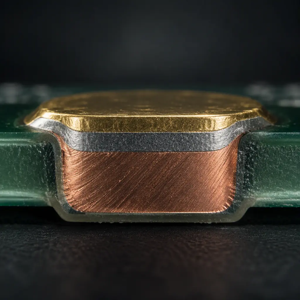
The name is misleading. Black pad is not a black pad in the way a burnt pad would be; it is a corrosion phenomenon at the interface between the electroless nickel layer and the immersion gold layer. During the immersion gold step, the gold deposition reaction is autocatalytic on nickel only if the nickel surface is active. If the nickel surface becomes passivated or the chemistry drifts, the gold bath does not just deposit gold — it begins to corrode the nickel beneath it. The result is a thin, porous, gold-rich layer sitting on top of a nickel surface that has been converted to a nickel oxide or a nickel-phosphorus compound that is electrically poor and mechanically weak.
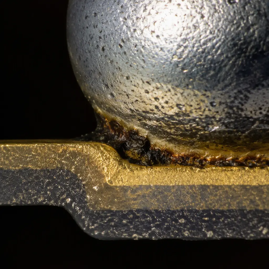
When solder is applied, the molten solder alloy must form an intermetallic compound with the nickel to create a proper joint. Where the nickel has been corroded, the intermetallic layer cannot form correctly. The solder balls up on a surface it cannot wet properly, or forms a thin, incomplete intermetallic that fractures under stress. The fracture runs along the corroded interface, which is why a black pad failure appears as a clean separation at the pad-joint boundary with a dark, grainy surface underneath — the black appearance that gave the defect its name.
Key Takeaway: Black pad is a nickel corrosion defect, not a soldering defect. If a joint fractures at the pad interface on an ENIG board, the first hypothesis should be that the nickel under the gold was compromised in the plating bath — not that the reflow profile was wrong.
The Chemistry Behind Black Pad
Understanding the chemistry is what separates a supplier who can prevent black pad from one who simply promises it will not happen. The electroless nickel step deposits a nickel-phosphorus alloy, typically 4–10% phosphorus. The immersion gold step then displaces a thin layer of nickel with gold through a galvanic exchange — the nickel dissolves into solution while gold deposits. This exchange is self-limiting: once a continuous gold layer forms, the nickel underneath is sealed from the bath and the reaction stops. Gold thickness is therefore inherently thin, typically 0.05–0.1 µm.
Black pad enters when the self-limiting behaviour breaks down. Three conditions drive it. First, an over-aggressive or contaminated immersion gold bath continues to attack the nickel through pores in the gold layer, producing a hyper-corrosion of the nickel surface. Second, insufficient or uneven electroless nickel deposition leaves a thin or porous nickel layer that the gold bath can penetrate. Third, a nickel bath with the wrong phosphorus content or excessive stabiliser produces a nickel surface that passivates and drives the gold bath into a corrosion regime. The common thread is that black pad is a process-window violation: when the bath chemistry sits where it should, the interface is sound; when it drifts out of window, the interface corrodes.
This is why gold thickness alone is not a sufficient specification. A common mistake is to demand a thick gold layer as protection, on the assumption that more gold means a better barrier. In practice, an over-thick immersion gold layer indicates an out-of-window bath that has been allowed to run too long or too hot — exactly the condition that produces black pad. The correct control is a gold thickness held within the ENIG specification (IPC-4552 places the range at 0.05–0.1 µm for immersion gold, sometimes quoted to 0.15 µm) plus verified nickel corrosion control, not simply "as much gold as possible."
How to Detect Black Pad Before It Reaches the Field
Black pad cannot be seen with the naked eye and rarely shows up on standard AOI, because AOI inspects the solder joint and the joint genuinely is there. Detection requires looking at the interface, which means either cross-sectioning the board or mechanically testing the joint to failure. Two methods are standard and they complement each other.
Microsection and SEM. A cross-section through a soldered pad is examined under a metallurgical microscope, and at higher magnification under a scanning electron microscope. A sound ENIG joint shows a well-formed layer of nickel-tin intermetallic (Ni3Sn4) between the solder and the nickel, typically 1–3 µm thick, with the bulk nickel intact beneath. A black-pad joint shows the intermetallic layer absent or discontinuous, a dark, etch-like corrosion zone at the nickel surface, and often a "mud-crack" texture in the gold-nickel region. The microsection is definitive because it shows the interface directly. The cost is that it is destructive and requires sample preparation, which is why it is used for qualification and failure analysis rather than 100% inspection. Our guide to microsection analysis covers how to read these cross-sections.
Ball shear and ball pull. A destructive mechanical test on assembled joints, typically on BGA or CSP balls. A ball is sheared laterally or pulled vertically and the fracture load recorded. A black-pad joint fails at a distinctly lower load than a good joint and — critically — fails at the pad interface rather than within the solder. The failure mode is as informative as the number: a ductile joint fails through the bulk solder, a black-pad joint fails cleanly at the pad with a rough, dark fracture surface. Ball shear per JESD22-B117 gives a quantifiable acceptance threshold; the interface failure location is the tell.
For a buyer, the practical takeaway is that neither method is part of a normal board inspection, so if black pad is a concern you must specify the test. A supplier who runs this test routinely for ENIG production has the data; a supplier who does not will only investigate after a field failure, which is the most expensive possible time.
Black Pad vs Other Brittle Fracture Causes
Not every brittle joint on an ENIG board is black pad, and misdiagnosing it sends corrective action in the wrong direction. Three other failure modes produce a fracture that can be mistaken for black pad, and the distinction matters because each has a different fix.
Excessive intermetallic growth is a thermal-history problem: too much time at temperature grows a thick, brittle copper-tin or nickel-tin intermetallic layer, and fracture occurs through that layer rather than along the pad interface. The fix is the reflow profile, not the plating. Solder contamination (for example, high levels of gold dissolved into the joint from thick gold plating, or lead contamination in a lead-free process) produces a joint that is brittle in the bulk rather than at the interface. The fix is process control at assembly. Mechanical overstress produces a fracture through the weakest cross-section, which may be the pad but usually with deformation evidence such as pad lifting or copper tearing. The fix is handling and mechanical design.
The distinguishing evidence is location and morphology. Black pad fractures sit precisely at the nickel-gold interface, show the dark corrosion zone under SEM, and occur even when the thermal profile and solder chemistry are nominal. If the fracture is elsewhere, or the interface looks clean under magnification, the cause is something else. This is why a fracture that is presumed to be black pad should always be confirmed by cross-section rather than accepted on the strength of the symptom alone.
Fabrication Controls That Prevent Black Pad
Prevention lives in the plating line, and the controls are well understood. A fabricator serious about ENIG reliability manages the following, and can show evidence of each when asked.
Hold gold thickness inside the spec, not above it
Immersion gold at 0.05–0.1 µm. An out-of-spec high reading signals an ageing bath and is a black-pad warning, not a bonus.
Control nickel phosphorus content
Typically 7–9% phosphorus for reliable ENIG. Too low or too high changes the corrosion behaviour of the nickel surface.
Maintain the immersion gold bath in window
Gold concentration, pH, temperature and immersion time all held to the chemistry supplier's window. Bath age and make-up logged.
Verify electroless nickel continuity
Uniform, pore-free nickel at adequate thickness before gold. A thin or porous nickel layer is an open door for the gold bath to corrode.
Run periodic microsection on ENIG lots
Regular cross-section checks catch interface corrosion before it becomes a shipped batch, turning a field failure into a line correction.
Provide plating thickness data with the lot
Nickel and gold thickness measured and reported. A supplier who cannot produce this is not controlling the process.
Key Takeaway: Black pad is prevented by keeping the electroless nickel and immersion gold baths inside their chemistry windows and verifying the interface periodically by cross-section — not by adding gold. Ask a supplier for the gold thickness range they hold and their nickel corrosion check method before you commit a high-reliability ENIG design.
Specifying ENIG So It Cannot Bite You
Beyond the fabrication controls, a buyer can write an ENIG specification that removes most of the risk. The specification should state the finish type as ENIG with reference to IPC-4552, name a gold thickness range rather than a minimum, require nickel thickness and phosphorus content to be declared, and — for high-reliability or high-value designs — require a microsection or ball shear report on the qualification lot. For the family of finishes and where ENIG sits relative to HASL, OSP, immersion silver and ENEPIG, see our comparison of ENIG versus HASL and the broader surface finish selection guide. A finish that is correct for the application removes an entire class of failure before it can start.
It is also worth matching the finish to the soldering process. Fine-pitch SMT with a flat pad requirement is exactly where ENIG earns its keep, but a design with unusual thermal demands or a very high-reliability joint may be better served by ENEPIG, which adds a palladium barrier layer between nickel and gold that resists the corrosion mechanism entirely. If black pad risk is a genuine concern for a critical design, ENEPIG is a legitimate mitigation, at higher cost.
Cost and Audit Implications for Buyers
The commercial reality of black pad is that the defect is cheap to prevent and extremely expensive to discover late. Preventing it costs good bath chemistry and periodic cross-section checks — routine operating cost for a competent ENIG line. Discovering it late costs a field failure, a recall or a costly screening exercise, because once boards are assembled there is no non-destructive way to identify which joints have a compromised interface. That asymmetry is the argument for treating ENIG process control as a qualification question rather than an inspection question.
When auditing a supplier for ENIG capability, the practical questions are: what gold thickness range do you hold, how do you monitor the immersion gold bath, what is your nickel phosphorus target, and can you provide a microsection or ball shear report for the qualification lot? A supplier with answers has the process under control. A supplier without them may still produce good boards most of the time — but black pad is precisely the failure that appears in the boards that are not most of the time. This is closely related to the general discipline described in our guide to incoming quality inspection and to the field-defect analysis in solder joint defects.
At Huaxing PCBA we run ENIG and ENEPIG finishes on fine-pitch production under IATF 16949 and ISO 9001, controlling gold thickness within spec and verifying the nickel interface by microsection, with thickness data and a free DFM review on every quote. Send your Gerber files with the finish specified and we will confirm the appropriate surface treatment and return a quote inside 24 hours, or talk to our engineering team about black pad risk on a high-reliability ENIG design.
